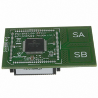
MA180025 Microchip Technology, MA180025 Datasheet - Page 173

MA180025
Manufacturer Part Number
MA180025
Description
MODULE PLUG-IN PIC18F87J90 PIM
Manufacturer
Microchip Technology
Series
PIC®r
Specifications of MA180025
Accessory Type
Plug-In Module (PIM) - PIC18F87J90
Product
Microcontroller Modules
Silicon Manufacturer
Microchip
Core Architecture
PIC
Core Sub-architecture
PIC18
Silicon Core Number
PIC18F
Silicon Family Name
PIC18FxxJxx
Lead Free Status / RoHS Status
Lead free / RoHS Compliant
For Use With/related Products
PICDEM LCD 2 Demonstration Board (DM163030)
For Use With
DM163030 - KIT DEV PICDEM LCD2
Lead Free Status / Rohs Status
Lead free / RoHS Compliant
Available stocks
Company
Part Number
Manufacturer
Quantity
Price
Company:
Part Number:
MA180025
Manufacturer:
Microchip Technology
Quantity:
135
Company:
Part Number:
MA180025
Manufacturer:
MICROCHIP
Quantity:
12 000
- Current page: 173 of 450
- Download datasheet (4Mb)
16.0
PIC18F87J90
(Capture/Compare/PWM) modules, designated CCP1
and CCP2. Both modules implement standard capture,
compare and Pulse-Width Modulation (PWM) modes.
REGISTER 16-1:
2010 Microchip Technology Inc.
bit 7
Legend:
R = Readable bit
-n = Value at POR
bit 7-6
bit 5-4
bit 3-0
Note 1:
U-0
—
CAPTURE/COMPARE/PWM
(CCP) MODULES
CCPxM<3:0> = 1011 will only reset the timer and not start an A/D conversion on a CCP1 match.
Unimplemented: Read as ‘0’
DCxB<1:0>: PWM Duty Cycle bit 1 and bit 0 for CCPx Module
Capture mode:
Unused.
Compare mode:
Unused.
PWM mode:
These bits are the two Least Significant bits (bit 1 and bit 0) of the 10-bit PWM duty cycle. The eight
Most Significant bits (DCx<9:2>) of the duty cycle are found in CCPRxL.
CCPxM<3:0>: CCPx Module Mode Select bits
0000 = Capture/Compare/PWM disabled (resets CCPx module)
0001 = Reserved
0010 = Compare mode, toggle output on match (CCPxIF bit is set)
0011 = Reserved
0100 = Capture mode, every falling edge
0101 = Capture mode, every rising edge
0110 = Capture mode, every 4th rising edge
0111 = Capture mode, every 16th rising edge
1000 = Compare mode: initialize CCPx pin low; on compare match, force CCPx pin high (CCPxIF bit
1001 = Compare mode: initialize CCPx pin high; on compare match, force CCPx pin low (CCPxIF bit
1010 = Compare mode: generate software interrupt on compare match (CCPxIF bit is set, CCPx pin
1011 = Compare mode: Special Event Trigger; reset timer; start A/D conversion on CCPx match
11xx = PWM mode
family
U-0
—
CCPxCON: CCPx CONTROL REGISTER (CCP1, CCP2 MODULES)
is set)
is set)
reflects I/O state)
(CCPxIF bit is set)
devices
W = Writable bit
‘1’ = Bit is set
DCxB1
R/W-0
have
(1)
two
DCxB0
R/W-0
CCP
U = Unimplemented bit, read as ‘0’
‘0’ = Bit is cleared
PIC18F87J90 FAMILY
CCPxM3
R/W-0
Each CCP module contains two 8-bit registers that can
operate as two 8-bit Capture registers, two 8-bit
Compare registers or two PWM Master/Slave Duty
Cycle registers. For the sake of clarity, all CCP module
operation in the following sections is described with
respect to CCP2, but is equally applicable to CCP1.
CCPxM2
R/W-0
x = Bit is unknown
CCPxM1
R/W-0
DS39933D-page 173
CCPxM0
R/W-0
bit 0
Related parts for MA180025
Image
Part Number
Description
Manufacturer
Datasheet
Request
R

Part Number:
Description:
Manufacturer:
Microchip Technology Inc.
Datasheet:

Part Number:
Description:
Manufacturer:
Microchip Technology Inc.
Datasheet:

Part Number:
Description:
Manufacturer:
Microchip Technology Inc.
Datasheet:

Part Number:
Description:
Manufacturer:
Microchip Technology Inc.
Datasheet:

Part Number:
Description:
Manufacturer:
Microchip Technology Inc.
Datasheet:

Part Number:
Description:
Manufacturer:
Microchip Technology Inc.
Datasheet:

Part Number:
Description:
Manufacturer:
Microchip Technology Inc.
Datasheet:

Part Number:
Description:
Manufacturer:
Microchip Technology Inc.
Datasheet:


