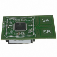
MA180025 Microchip Technology, MA180025 Datasheet - Page 189

MA180025
Manufacturer Part Number
MA180025
Description
MODULE PLUG-IN PIC18F87J90 PIM
Manufacturer
Microchip Technology
Series
PIC®r
Specifications of MA180025
Accessory Type
Plug-In Module (PIM) - PIC18F87J90
Product
Microcontroller Modules
Silicon Manufacturer
Microchip
Core Architecture
PIC
Core Sub-architecture
PIC18
Silicon Core Number
PIC18F
Silicon Family Name
PIC18FxxJxx
Lead Free Status / RoHS Status
Lead free / RoHS Compliant
For Use With/related Products
PICDEM LCD 2 Demonstration Board (DM163030)
For Use With
DM163030 - KIT DEV PICDEM LCD2
Lead Free Status / Rohs Status
Lead free / RoHS Compliant
Available stocks
Company
Part Number
Manufacturer
Quantity
Price
Company:
Part Number:
MA180025
Manufacturer:
Microchip Technology
Quantity:
135
Company:
Part Number:
MA180025
Manufacturer:
MICROCHIP
Quantity:
12 000
- Current page: 189 of 450
- Download datasheet (4Mb)
17.3
The LCD driver module is capable of generating the
required bias voltages for LCD operation with a mini-
mum of external components. This includes the ability
to generate the different voltage levels required by the
different bias types that are required by the LCD. The
driver module can also provide bias voltages, both
above and below microcontroller V
of an on-chip LCD voltage regulator.
17.3.1
PIC18F87J90 family devices support three bias types
based on the waveforms generated to control
segments and commons:
• Static (two discrete levels)
• 1/2 Bias (three discrete levels
• 1/3 Bias (four discrete levels)
The use of different waveforms in driving the LCD is dis-
cussed in more detail in Section 17.8 “LCD Waveform
Generation”.
REGISTER 17-5:
2010 Microchip Technology Inc.
bit 7
Legend:
R = Readable bit
-n = Value at POR
bit 7
bit 6
bit 5-3
bit 2
bit 1-0
U-0
—
LCD Bias Generation
LCD BIAS TYPES
Unimplemented: Read as ‘0’
CPEN: LCD Charge Pump Enable bit
1 = Charge pump enabled; highest LCD bias voltage is 3.6V
0 = Charge pump disabled; highest LCD bias voltage is AV
BIAS<2:0>: Regulator Voltage Output Control bits
111 = 3.60V peak (offset on LCDBIAS0 of 0V)
110 = 3.47V peak (offset on LCDBIAS0 of 0.13V)
101 = 3.34V peak (offset on LCDBIAS0 of 0.26V)
100 = 3.21V peak (offset on LCDBIAS0 of 0.39V)
011 = 3.08V peak (offset on LCDBIAS0 of 0.52V)
010 = 2.95V peak (offset on LCDBIAS0 of 0.65V)
001 = 2.82V peak (offset on LCDBIAS0 of 0.78V)
000 = 2.69V peak (offset on LCDBIAS0 of 0.91V)
MODE13: 1/3 LCD Bias Enable bit
1 = Regulator output supports 1/3 LCD Bias mode
0 = Regulator output supports static LCD Bias mode
CKSEL<1:0>: Regulator Clock Source Select bits
11 = INTRC
10 = INTOSC 8 MHz source
01 = Timer1 oscillator
00 = LCD regulator disabled
CPEN
RW-0
LCDREG: VOLTAGE REGULATOR CONTROL REGISTER
W = Writable bit
‘1’ = Bit is set
BIAS2
RW-1
DD
, through the use
BIAS1
RW-1
U = Unimplemented bit, read as ‘0’
‘0’ = Bit is cleared
PIC18F87J90 FAMILY
BIAS0
17.3.2
The purpose of the LCD regulator is to provide proper
bias voltage and good contrast for the LCD, regardless
of V
internal voltage reference. The regulator can be config-
ured by using external components to boost bias
voltage above V
constant voltage below V
selectively disabled to allow bias voltages to be
generated by an external resistor network.
The LCD regulator is controlled through the LCDREG
register (Register 17-5). It is enabled or disabled using
the CKSEL<1:0> bits, while the charge pump can be
selectively enabled using the CPEN bit. When the reg-
ulator is enabled, the MODE13 bit is used to select the
bias type. The peak LCD bias voltage, measured as a
difference between the potentials of LCDBIAS3 and
LCDBIAS0, is configured with the BIAS bits.
RW-1
DD
levels. This module contains a charge pump and
DD
LCD VOLTAGE REGULATOR
MODE13
RW-1
DD
. It can also operate a display at a
DD
x = Bit is unknown
. The regulator can also be
CKSEL1
RW-0
DS39933D-page 189
CKSEL0
RW-0
bit 0
Related parts for MA180025
Image
Part Number
Description
Manufacturer
Datasheet
Request
R

Part Number:
Description:
Manufacturer:
Microchip Technology Inc.
Datasheet:

Part Number:
Description:
Manufacturer:
Microchip Technology Inc.
Datasheet:

Part Number:
Description:
Manufacturer:
Microchip Technology Inc.
Datasheet:

Part Number:
Description:
Manufacturer:
Microchip Technology Inc.
Datasheet:

Part Number:
Description:
Manufacturer:
Microchip Technology Inc.
Datasheet:

Part Number:
Description:
Manufacturer:
Microchip Technology Inc.
Datasheet:

Part Number:
Description:
Manufacturer:
Microchip Technology Inc.
Datasheet:

Part Number:
Description:
Manufacturer:
Microchip Technology Inc.
Datasheet:


