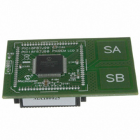
MA180025 Microchip Technology, MA180025 Datasheet - Page 41

MA180025
Manufacturer Part Number
MA180025
Description
MODULE PLUG-IN PIC18F87J90 PIM
Manufacturer
Microchip Technology
Series
PIC®r
Specifications of MA180025
Accessory Type
Plug-In Module (PIM) - PIC18F87J90
Product
Microcontroller Modules
Silicon Manufacturer
Microchip
Core Architecture
PIC
Core Sub-architecture
PIC18
Silicon Core Number
PIC18F
Silicon Family Name
PIC18FxxJxx
Lead Free Status / RoHS Status
Lead free / RoHS Compliant
For Use With/related Products
PICDEM LCD 2 Demonstration Board (DM163030)
For Use With
DM163030 - KIT DEV PICDEM LCD2
Lead Free Status / Rohs Status
Lead free / RoHS Compliant
Available stocks
Company
Part Number
Manufacturer
Quantity
Price
Company:
Part Number:
MA180025
Manufacturer:
Microchip Technology
Quantity:
135
Company:
Part Number:
MA180025
Manufacturer:
MICROCHIP
Quantity:
12 000
- Current page: 41 of 450
- Download datasheet (4Mb)
3.5
The PIC18F87J90 family of devices includes an
internal oscillator block which generates two different
clock signals; either can be used as the micro-
controller’s clock source. This may eliminate the need
for an external oscillator circuit on the OSC1 and/or
OSC2 pins.
The main output is the Fast RC oscillator or INTOSC,
an 8 MHz clock source which can be used to directly
drive the device clock. It also drives a postscaler, which
can provide a range of clock frequencies from 31 kHz
to 4 MHz. INTOSC is enabled when a clock frequency
from 125 kHz to 8 MHz is selected. The INTOSC out-
put can also be enabled when 31 kHz is selected,
depending on the INTSRC bit (OSCTUNE<7>).
The other clock source is the Internal RC oscillator
(INTRC), which provides a nominal 31 kHz output.
INTRC is enabled if it is selected as the device clock
source; it is also enabled automatically when any of the
following are enabled:
• Power-up Timer
• Fail-Safe Clock Monitor
• Watchdog Timer
• Two-Speed Start-up
These features are discussed in greater detail in
Section 25.0 “Special Features of the CPU”.
The clock source frequency (INTOSC direct, INTOSC
with postscaler or INTRC direct) is selected by config-
uring the IRCF bits of the OSCCON register. The
default frequency on device Resets is 4 MHz.
3.5.1
Using the internal oscillator as the clock source elimi-
nates the need for up to two external oscillator pins,
which can then be used for digital I/O. Two distinct
oscillator configurations, which are determined by the
FOSC Configuration bits, are available:
• In INTIO1 mode, the OSC2 pin outputs F
• In INTIO2 mode, OSC1 functions as RA7 and
2010 Microchip Technology Inc.
while OSC1 functions as RA7 (see Figure 3-6) for
digital input and output.
OSC2 functions as RA6 (see Figure 3-7), both for
digital input and output.
Internal Oscillator Block
INTIO MODES
OSC
/4,
PIC18F87J90 FAMILY
FIGURE 3-6:
FIGURE 3-7:
3.5.2
The 4x Phase Locked Loop (PLL) can be used with the
internal oscillator block to produce faster device clock
speeds than are normally possible with the internal
oscillator sources. When enabled, the PLL produces a
clock speed of 16 MHz or 32 MHz.
PLL operation is controlled through software. The con-
trol bit, PLLEN (OSCTUNE<6>), is used to enable or
disable its operation. The PLL is available only to
INTOSC when the device is configured to use one of
the INTPLL modes as the primary clock source
(FOSC<2:0> = 011 or 001). Additionally, the PLL will
only function when the selected output frequency is
either 4 MHz or 8 MHz (OSCCON<6:4> = 111 or 110).
Like the INTIO modes, there are two distinct INTPLL
modes available:
• In INTPLL1 mode, the OSC2 pin outputs F
• In INTPLL2 mode, OSC1 functions as RA7 and
while OSC1 functions as RA7 for digital input and
output. Externally, this is identical in appearance
to INTIO1 (Figure 3-6).
OSC2 functions as RA6, both for digital input and
output. Externally, this is identical to INTIO2
(Figure 3-7).
F
RA7
RA6
OSC
RA7
/4
INTPLL MODES
INTIO1 OSCILLATOR MODE
INTIO2 OSCILLATOR MODE
I/O (OSC1)
I/O (OSC2)
I/O (OSC1)
OSC2
PIC18F87J90
PIC18F87J90
DS39933D-page 41
OSC
/4,
Related parts for MA180025
Image
Part Number
Description
Manufacturer
Datasheet
Request
R

Part Number:
Description:
Manufacturer:
Microchip Technology Inc.
Datasheet:

Part Number:
Description:
Manufacturer:
Microchip Technology Inc.
Datasheet:

Part Number:
Description:
Manufacturer:
Microchip Technology Inc.
Datasheet:

Part Number:
Description:
Manufacturer:
Microchip Technology Inc.
Datasheet:

Part Number:
Description:
Manufacturer:
Microchip Technology Inc.
Datasheet:

Part Number:
Description:
Manufacturer:
Microchip Technology Inc.
Datasheet:

Part Number:
Description:
Manufacturer:
Microchip Technology Inc.
Datasheet:

Part Number:
Description:
Manufacturer:
Microchip Technology Inc.
Datasheet:


