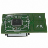
MA180025 Microchip Technology, MA180025 Datasheet - Page 206

MA180025
Manufacturer Part Number
MA180025
Description
MODULE PLUG-IN PIC18F87J90 PIM
Manufacturer
Microchip Technology
Series
PIC®r
Specifications of MA180025
Accessory Type
Plug-In Module (PIM) - PIC18F87J90
Product
Microcontroller Modules
Silicon Manufacturer
Microchip
Core Architecture
PIC
Core Sub-architecture
PIC18
Silicon Core Number
PIC18F
Silicon Family Name
PIC18FxxJxx
Lead Free Status / RoHS Status
Lead free / RoHS Compliant
For Use With/related Products
PICDEM LCD 2 Demonstration Board (DM163030)
For Use With
DM163030 - KIT DEV PICDEM LCD2
Lead Free Status / Rohs Status
Lead free / RoHS Compliant
Available stocks
Company
Part Number
Manufacturer
Quantity
Price
Company:
Part Number:
MA180025
Manufacturer:
Microchip Technology
Quantity:
135
Company:
Part Number:
MA180025
Manufacturer:
MICROCHIP
Quantity:
12 000
- Current page: 206 of 450
- Download datasheet (4Mb)
PIC18F87J90 FAMILY
17.9
The LCD timing generation provides an interrupt that
defines the LCD frame timing. This interrupt can be
used to coordinate the writing of the pixel data with the
start of a new frame. Writing pixel data at the frame
boundary allows a visually crisp transition of the image.
This interrupt can also be used to synchronize external
events to the LCD. For example, the interface to an
external segment driver can be synchronized for a
segment data update to the LCD frame.
A new frame is defined to begin at the leading edge of
the COM0 common signal. The interrupt will be set
immediately after the LCD controller completes
accessing all pixel data required for a frame. This will
occur at a fixed interval before the frame boundary
(T
will begin to access data for the next frame within the
interval from the interrupt to when the controller begins
to access data after the interrupt (T
must be written within T
controller will begin to access the data for the next
frame.
FIGURE 17-17:
DS39933D-page 206
FINT
T
T
), as shown in Figure 17-17. The LCD controller
COM0
COM1
COM2
COM3
FWR
FINT
LCD Interrupts
= T
= (T
(T
FRAME
FWR
FWR
/2 – (2 T
/2 – (1 T
Boundary
/2 * (LMUX<1:0> + 1) + T
Frame
EXAMPLE WAVEFORMS AND INTERRUPT TIMING
IN QUARTER DUTY CYCLE DRIVE
FWR
CY
CY
, as this is when the LCD
+ 40 ns)) Minimum = 1.5(T
+ 40 ns)) Maximum = 1.5(T
FWR
). New data
CY
/2
2 Frames
FRAME
FRAME
Boundary
Frame
/4) – (2 T
/4) – (1 T
When the LCD driver is running with Type-B wave-
forms, and the LMUX<1:0> bits are not equal to ‘00’,
there are some additional issues that must be
addressed. Since the DC voltage on the pixel takes two
frames to maintain zero volts, the pixel data must not
change between subsequent frames. If the pixel data
was allowed to change, the waveform for the odd
frames would not necessarily be the complement of the
waveform generated in the even frames and a DC
component would be introduced into the panel. There-
fore, when using Type-B waveforms, the user must
synchronize the LCD pixel updates to occur within a
subframe after the frame interrupt.
To correctly sequence writing while in Type-B, the
interrupt will only occur on complete phase intervals. If
the user attempts to write when the write is disabled,
the WERR (LCDCON<5>) bit is set.
Note:
CY
CY
LCD
Interrupt
Occurs
+ 40 ns)
+ 40 ns)
The interrupt is not generated when the
Type-A waveform is selected and when the
Type-B with no multiplex (static) is
selected.
T
FWR
T
FINT
2010 Microchip Technology Inc.
Controller Accesses
Next Frame Data
Boundary
Frame
V
V
V
V
V
V
V
V
V
V
V
V
V
V
V
V
3
2
1
0
3
2
1
0
3
2
1
0
3
2
1
0
Related parts for MA180025
Image
Part Number
Description
Manufacturer
Datasheet
Request
R

Part Number:
Description:
Manufacturer:
Microchip Technology Inc.
Datasheet:

Part Number:
Description:
Manufacturer:
Microchip Technology Inc.
Datasheet:

Part Number:
Description:
Manufacturer:
Microchip Technology Inc.
Datasheet:

Part Number:
Description:
Manufacturer:
Microchip Technology Inc.
Datasheet:

Part Number:
Description:
Manufacturer:
Microchip Technology Inc.
Datasheet:

Part Number:
Description:
Manufacturer:
Microchip Technology Inc.
Datasheet:

Part Number:
Description:
Manufacturer:
Microchip Technology Inc.
Datasheet:

Part Number:
Description:
Manufacturer:
Microchip Technology Inc.
Datasheet:


