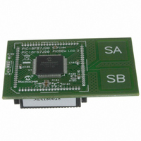
MA180025 Microchip Technology, MA180025 Datasheet - Page 143

MA180025
Manufacturer Part Number
MA180025
Description
MODULE PLUG-IN PIC18F87J90 PIM
Manufacturer
Microchip Technology
Series
PIC®r
Specifications of MA180025
Accessory Type
Plug-In Module (PIM) - PIC18F87J90
Product
Microcontroller Modules
Silicon Manufacturer
Microchip
Core Architecture
PIC
Core Sub-architecture
PIC18
Silicon Core Number
PIC18F
Silicon Family Name
PIC18FxxJxx
Lead Free Status / RoHS Status
Lead free / RoHS Compliant
For Use With/related Products
PICDEM LCD 2 Demonstration Board (DM163030)
For Use With
DM163030 - KIT DEV PICDEM LCD2
Lead Free Status / Rohs Status
Lead free / RoHS Compliant
Available stocks
Company
Part Number
Manufacturer
Quantity
Price
Company:
Part Number:
MA180025
Manufacturer:
Microchip Technology
Quantity:
135
Company:
Part Number:
MA180025
Manufacturer:
MICROCHIP
Quantity:
12 000
- Current page: 143 of 450
- Download datasheet (4Mb)
12.0
The Timer1 timer/counter module incorporates these
features:
• Software selectable operation as a 16-bit timer or
• Readable and writable 8-bit registers (TMR1H
• Selectable clock source (internal or external) with
• Interrupt-on-overflow
• Reset on CCP Special Event Trigger
• Device clock status flag (T1RUN)
REGISTER 12-1:
2010 Microchip Technology Inc.
bit 7
Legend:
R = Readable bit
-n = Value at POR
bit 7
bit 6
bit 5-4
bit 3
bit 2
bit 1
bit 0
counter
and TMR1L)
device clock or Timer1 oscillator internal options
R/W-0
RD16
TIMER1 MODULE
RD16: 16-Bit Read/Write Mode Enable bit
1 = Enables register read/write of TImer1 in one 16-bit operation
0 = Enables register read/write of Timer1 in two 8-bit operations
T1RUN: Timer1 System Clock Status bit
1 = Device clock is derived from Timer1 oscillator
0 = Device clock is derived from another source
T1CKPS<1:0>: Timer1 Input Clock Prescale Select bits
11 = 1:8 Prescale value
10 = 1:4 Prescale value
01 = 1:2 Prescale value
00 = 1:1 Prescale value
T1OSCEN: Timer1 Oscillator Enable bit
1 = Timer1 oscillator is enabled
0 = Timer1 oscillator is shut off
The oscillator inverter and feedback resistor are turned off to eliminate power drain.
T1SYNC: Timer1 External Clock Input Synchronization Select bit
When TMR1CS = 1:
1 = Do not synchronize external clock input
0 = Synchronize external clock input
When TMR1CS = 0:
This bit is ignored. Timer1 uses the internal clock when TMR1CS = 0.
TMR1CS: Timer1 Clock Source Select bit
1 = External clock from pin RC0/T1OSO/T13CKI (on the rising edge)
0 = Internal clock (F
TMR1ON: Timer1 On bit
1 = Enables Timer1
0 = Stops Timer1
T1RUN
R-0
T1CON: TIMER1 CONTROL REGISTER
W = Writable bit
‘1’ = Bit is set
T1CKPS1
R/W-0
OSC
/4)
T1CKPS0
R/W-0
U = Unimplemented bit, read as ‘0’
‘0’ = Bit is cleared
T1OSCEN
PIC18F87J90 FAMILY
R/W-0
A simplified block diagram of the Timer1 module is
shown in Figure 12-1. A block diagram of the module’s
operation in Read/Write mode is shown in Figure 12-2.
The module incorporates its own low-power oscillator
to provide an additional clocking option. The Timer1
oscillator can also be used as a low-power clock source
for the microcontroller in power-managed operation.
Timer1 can also be used to provide Real-Time Clock
(RTC) functionality to applications with only a minimal
addition of external components and code overhead.
Timer1 is controlled through the T1CON Control
register (Register 12-1). It also contains the Timer1
Oscillator Enable bit (T1OSCEN). Timer1 can be
enabled or disabled by setting or clearing control bit,
TMR1ON (T1CON<0>).
T1SYNC
R/W-0
x = Bit is unknown
TMR1CS
R/W-0
DS39933D-page 143
TMR1ON
R/W-0
bit 0
Related parts for MA180025
Image
Part Number
Description
Manufacturer
Datasheet
Request
R

Part Number:
Description:
Manufacturer:
Microchip Technology Inc.
Datasheet:

Part Number:
Description:
Manufacturer:
Microchip Technology Inc.
Datasheet:

Part Number:
Description:
Manufacturer:
Microchip Technology Inc.
Datasheet:

Part Number:
Description:
Manufacturer:
Microchip Technology Inc.
Datasheet:

Part Number:
Description:
Manufacturer:
Microchip Technology Inc.
Datasheet:

Part Number:
Description:
Manufacturer:
Microchip Technology Inc.
Datasheet:

Part Number:
Description:
Manufacturer:
Microchip Technology Inc.
Datasheet:

Part Number:
Description:
Manufacturer:
Microchip Technology Inc.
Datasheet:


