DF2328BVF25V Renesas Electronics America, DF2328BVF25V Datasheet - Page 112
DF2328BVF25V
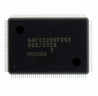
Manufacturer Part Number
DF2328BVF25V
Description
IC H8S MCU FLASH 256K 128QFP
Manufacturer
Renesas Electronics America
Series
H8® H8S/2300r
Datasheets
1.HEWH8E10A.pdf
(19 pages)
2.D12312SVTE25V.pdf
(341 pages)
3.D12322RVF25V.pdf
(1304 pages)
Specifications of DF2328BVF25V
Core Processor
H8S/2000
Core Size
16-Bit
Speed
25MHz
Connectivity
SCI, SmartCard
Peripherals
DMA, POR, PWM, WDT
Number Of I /o
87
Program Memory Size
256KB (256K x 8)
Program Memory Type
FLASH
Ram Size
8K x 8
Voltage - Supply (vcc/vdd)
2.7 V ~ 3.6 V
Data Converters
A/D 8x10b; D/A 2x8b
Oscillator Type
Internal
Operating Temperature
-20°C ~ 75°C
Package / Case
128-QFP
For Use With
EDK2329 - DEV EVALUATION KIT H8S/2329
Lead Free Status / RoHS Status
Lead free / RoHS Compliant
Eeprom Size
-
Other names
HD64F2328BVF25V
Available stocks
Company
Part Number
Manufacturer
Quantity
Price
Company:

Part Number:
DF2328BVF25V
Manufacturer:
Renesas Electronics America
Quantity:
10 000


Section 3 MCU Operating Modes
3.1.3
The H8S/2329 Group and H8S/2328 Group have a mode control register (MDCR) that indicates
the inputs at the mode pins (MD
control register 2 (SYSCR2) *
registers.
Table 3.3
Name
Mode control register
System control register
System control register 2 *
Notes: 1. Lower 16 bits of the address.
3.2
3.2.1
Note: * Determined by pins MD
MDCR is an 8-bit read-only register that indicates the current operating mode of the H8S/2329
Group and H8S/2328 Group chip.
Bit 7—Reserved: This bit is always read as 1, and cannot be modified.
Bits 6 to 3—Reserved: These bits are always read as 0, and cannot be modified.
Bits 2 to 0—Mode Select 2 to 0 (MDS2 to MDS0): These bits indicate the input levels at pins
MD
MDS2 to MDS0 are read-only bits, and cannot be written to. The mode pin (MD
levels are latched into these bits when MDCR is read. These latches are canceled by a reset.
Rev.6.00 Sep. 27, 2007 Page 80 of 1268
REJ09B0220-0600
Bit
Initial value :
R/W
2
to MD
2. The SYSCR2 register can only be used in the F-ZTAT versions. In the mask ROM and
Register Configuration
Register Descriptions
Mode Control Register (MDCR)
ROMless versions this register will return an undefined value if read, and cannot be
modified.
0
Registers
(the current operating mode). Bits MDS2 to MDS0 correspond to pins MD
:
:
—
—
7
1
2
2
—
—
2
6
0
that control the operation of the chip. Table 3.3 summarizes these
Abbreviation
MDCR
SYSCR
SYSCR2
2
to MD
to MD
0
.
0
—
—
), and a system control register (SYSCR) and a system
5
0
R/W
R/W
R
R/W
—
—
4
0
—
—
3
0
Initial Value
Undefined
H'01
H'00
MDS2
— *
R
2
MDS1
2
Address *
H'FF3B
H'FF39
H'FF42
— *
to MD
R
1
2
0
) input
to MD
MDS0
1
— *
R
0
0
.
Related parts for DF2328BVF25V
Image
Part Number
Description
Manufacturer
Datasheet
Request
R

Part Number:
Description:
KIT STARTER FOR M16C/29
Manufacturer:
Renesas Electronics America
Datasheet:

Part Number:
Description:
KIT STARTER FOR R8C/2D
Manufacturer:
Renesas Electronics America
Datasheet:

Part Number:
Description:
R0K33062P STARTER KIT
Manufacturer:
Renesas Electronics America
Datasheet:

Part Number:
Description:
KIT STARTER FOR R8C/23 E8A
Manufacturer:
Renesas Electronics America
Datasheet:

Part Number:
Description:
KIT STARTER FOR R8C/25
Manufacturer:
Renesas Electronics America
Datasheet:

Part Number:
Description:
KIT STARTER H8S2456 SHARPE DSPLY
Manufacturer:
Renesas Electronics America
Datasheet:

Part Number:
Description:
KIT STARTER FOR R8C38C
Manufacturer:
Renesas Electronics America
Datasheet:

Part Number:
Description:
KIT STARTER FOR R8C35C
Manufacturer:
Renesas Electronics America
Datasheet:

Part Number:
Description:
KIT STARTER FOR R8CL3AC+LCD APPS
Manufacturer:
Renesas Electronics America
Datasheet:
Part Number:
Description:
KIT STARTER FOR RX610
Manufacturer:
Renesas Electronics America
Datasheet:

Part Number:
Description:
KIT STARTER FOR R32C/118
Manufacturer:
Renesas Electronics America
Datasheet:

Part Number:
Description:
KIT DEV RSK-R8C/26-29
Manufacturer:
Renesas Electronics America
Datasheet:

Part Number:
Description:
KIT STARTER FOR SH7124
Manufacturer:
Renesas Electronics America
Datasheet:

Part Number:
Description:
KIT STARTER FOR H8SX/1622
Manufacturer:
Renesas Electronics America
Datasheet:

Part Number:
Description:
KIT DEV FOR SH7203
Manufacturer:
Renesas Electronics America
Datasheet: