DF2328BVF25V Renesas Electronics America, DF2328BVF25V Datasheet - Page 945
DF2328BVF25V
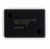
Manufacturer Part Number
DF2328BVF25V
Description
IC H8S MCU FLASH 256K 128QFP
Manufacturer
Renesas Electronics America
Series
H8® H8S/2300r
Datasheets
1.HEWH8E10A.pdf
(19 pages)
2.D12312SVTE25V.pdf
(341 pages)
3.D12322RVF25V.pdf
(1304 pages)
Specifications of DF2328BVF25V
Core Processor
H8S/2000
Core Size
16-Bit
Speed
25MHz
Connectivity
SCI, SmartCard
Peripherals
DMA, POR, PWM, WDT
Number Of I /o
87
Program Memory Size
256KB (256K x 8)
Program Memory Type
FLASH
Ram Size
8K x 8
Voltage - Supply (vcc/vdd)
2.7 V ~ 3.6 V
Data Converters
A/D 8x10b; D/A 2x8b
Oscillator Type
Internal
Operating Temperature
-20°C ~ 75°C
Package / Case
128-QFP
For Use With
EDK2329 - DEV EVALUATION KIT H8S/2329
Lead Free Status / RoHS Status
Lead free / RoHS Compliant
Eeprom Size
-
Other names
HD64F2328BVF25V
Available stocks
Company
Part Number
Manufacturer
Quantity
Price
Company:

Part Number:
DF2328BVF25V
Manufacturer:
Renesas Electronics America
Quantity:
10 000


Bit 5—Division Ratio Select (DIV): When the DIV bit is set to 1, the medium-speed mode is
disabled and a clock obtained using the division ratio set with bits SCK2 to SCK0 is supplied to
the entire chip. In this way, the current dissipation within the chip is reduced in proportion to the
division ratio. As the frequency of φ changes, the following points must be noted.
• The division ratio set with bits SCK2 to SCK0 should be selected so as to fall within the
• All internal modules basically operate on φ. Note, therefore, that time processing involving the
• The division ratio can be changed while the chip is operating. The clock output from the φ pin
• Do not set the DIV bit and bits SCK2 to SCK0 simultaneously. First set the DIV bit, then bits
Bit 5
DIV
0
1
Bits 4 and 3—Reserved: These bits cannot be modified and are always read as 0.
Bits 2 to 0—System Clock Select 2 to 0 (SCK2 to SCK0): When the DIV bit is cleared to 0,
these bits select the medium-speed mode; when the DIV bit is set to 1, they select the division
ratio of the clock supplied to the entire chip.
guaranteed operation range of clock cycle time tcyc given in the AC timing table in the
Electrical Characteristics section. Ensure that φ min = 2 MHz, and the condition φ < 2 MHz
does not arise.
timers, the SCI, etc., will change when the division ratio changes. The wait time when software
standby is cleared will also change in line with a change in the division ratio.
will also change when the division ratio is changed. The frequency of the clock output from
the φ pin in this case will be as follows:
Where:
SCK2 to SCK0.
Description
When bits SCK2 to SCK0 are set to other than high-speed mode, medium-speed
mode is set
When bits SCK2 to SCK0 are set to other than high-speed mode, a divided clock is
supplied to the entire chip
φ = EXTAL × n
EXTAL: Crystal resonator or external clock frequency
n:
Division ratio (n = φ/2, φ/4, or φ/8)
Rev.6.00 Sep. 27, 2007 Page 913 of 1268
Section 20 Clock Pulse Generator
REJ09B0220-0600
(Initial value)
Related parts for DF2328BVF25V
Image
Part Number
Description
Manufacturer
Datasheet
Request
R

Part Number:
Description:
KIT STARTER FOR M16C/29
Manufacturer:
Renesas Electronics America
Datasheet:

Part Number:
Description:
KIT STARTER FOR R8C/2D
Manufacturer:
Renesas Electronics America
Datasheet:

Part Number:
Description:
R0K33062P STARTER KIT
Manufacturer:
Renesas Electronics America
Datasheet:

Part Number:
Description:
KIT STARTER FOR R8C/23 E8A
Manufacturer:
Renesas Electronics America
Datasheet:

Part Number:
Description:
KIT STARTER FOR R8C/25
Manufacturer:
Renesas Electronics America
Datasheet:

Part Number:
Description:
KIT STARTER H8S2456 SHARPE DSPLY
Manufacturer:
Renesas Electronics America
Datasheet:

Part Number:
Description:
KIT STARTER FOR R8C38C
Manufacturer:
Renesas Electronics America
Datasheet:

Part Number:
Description:
KIT STARTER FOR R8C35C
Manufacturer:
Renesas Electronics America
Datasheet:

Part Number:
Description:
KIT STARTER FOR R8CL3AC+LCD APPS
Manufacturer:
Renesas Electronics America
Datasheet:
Part Number:
Description:
KIT STARTER FOR RX610
Manufacturer:
Renesas Electronics America
Datasheet:

Part Number:
Description:
KIT STARTER FOR R32C/118
Manufacturer:
Renesas Electronics America
Datasheet:

Part Number:
Description:
KIT DEV RSK-R8C/26-29
Manufacturer:
Renesas Electronics America
Datasheet:

Part Number:
Description:
KIT STARTER FOR SH7124
Manufacturer:
Renesas Electronics America
Datasheet:

Part Number:
Description:
KIT STARTER FOR H8SX/1622
Manufacturer:
Renesas Electronics America
Datasheet:

Part Number:
Description:
KIT DEV FOR SH7203
Manufacturer:
Renesas Electronics America
Datasheet: