DF2328BVF25V Renesas Electronics America, DF2328BVF25V Datasheet - Page 710
DF2328BVF25V
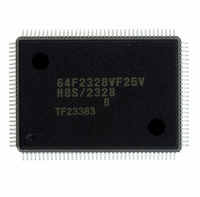
Manufacturer Part Number
DF2328BVF25V
Description
IC H8S MCU FLASH 256K 128QFP
Manufacturer
Renesas Electronics America
Series
H8® H8S/2300r
Datasheets
1.HEWH8E10A.pdf
(19 pages)
2.D12312SVTE25V.pdf
(341 pages)
3.D12322RVF25V.pdf
(1304 pages)
Specifications of DF2328BVF25V
Core Processor
H8S/2000
Core Size
16-Bit
Speed
25MHz
Connectivity
SCI, SmartCard
Peripherals
DMA, POR, PWM, WDT
Number Of I /o
87
Program Memory Size
256KB (256K x 8)
Program Memory Type
FLASH
Ram Size
8K x 8
Voltage - Supply (vcc/vdd)
2.7 V ~ 3.6 V
Data Converters
A/D 8x10b; D/A 2x8b
Oscillator Type
Internal
Operating Temperature
-20°C ~ 75°C
Package / Case
128-QFP
For Use With
EDK2329 - DEV EVALUATION KIT H8S/2329
Lead Free Status / RoHS Status
Lead free / RoHS Compliant
Eeprom Size
-
Other names
HD64F2328BVF25V
Available stocks
Company
Part Number
Manufacturer
Quantity
Price
Company:

Part Number:
DF2328BVF25V
Manufacturer:
Renesas Electronics America
Quantity:
10 000


Section 15 Smart Card Interface
15.3
15.3.1
The main functions of the smart card interface are as follows.
• One frame consists of 8-bit data plus a parity bit.
• In transmission, a guard time of at least 2 etu (1 etu in block transfer mode) (elementary time
• If a parity error is detected during reception, a low error signal level is output for one etu
• If the error signal is sampled during transmission, the same data is transmitted automatically
• Only asynchronous communication is supported; there is no synchronous communication
15.3.2
Figure 15.2 shows a schematic diagram of smart card interface related pin connections.
In communication with an IC card, since both transmission and reception are carried out on a
single data communication line, the chip’s TxD pin and RxD pin should both be connected to the
line, as shown in the figure. The data communication line should be pulled up to the V
supply with a resistor.
When the clock generated on the smart card interface is used by an IC card, the SCK pin output is
input to the CLK pin of the IC card. No connection is needed if the IC card uses an internal clock.
Chip port output is used as the reset signal.
Other pins must normally be connected to the power supply or ground.
Rev.6.00 Sep. 27, 2007 Page 678 of 1268
REJ09B0220-0600
unit: the time for transfer of 1 bit) is left between the end of the parity bit and the start of the
next frame.
period, 10.5 etu after the start bit. (This does not apply to block transfer mode.)
after the elapse of 2 etu or longer. (This does not apply to block transfer mode.)
function.
Overview
Pin Connections
Operation
CC
power
Related parts for DF2328BVF25V
Image
Part Number
Description
Manufacturer
Datasheet
Request
R

Part Number:
Description:
KIT STARTER FOR M16C/29
Manufacturer:
Renesas Electronics America
Datasheet:

Part Number:
Description:
KIT STARTER FOR R8C/2D
Manufacturer:
Renesas Electronics America
Datasheet:

Part Number:
Description:
R0K33062P STARTER KIT
Manufacturer:
Renesas Electronics America
Datasheet:

Part Number:
Description:
KIT STARTER FOR R8C/23 E8A
Manufacturer:
Renesas Electronics America
Datasheet:

Part Number:
Description:
KIT STARTER FOR R8C/25
Manufacturer:
Renesas Electronics America
Datasheet:

Part Number:
Description:
KIT STARTER H8S2456 SHARPE DSPLY
Manufacturer:
Renesas Electronics America
Datasheet:

Part Number:
Description:
KIT STARTER FOR R8C38C
Manufacturer:
Renesas Electronics America
Datasheet:

Part Number:
Description:
KIT STARTER FOR R8C35C
Manufacturer:
Renesas Electronics America
Datasheet:

Part Number:
Description:
KIT STARTER FOR R8CL3AC+LCD APPS
Manufacturer:
Renesas Electronics America
Datasheet:
Part Number:
Description:
KIT STARTER FOR RX610
Manufacturer:
Renesas Electronics America
Datasheet:

Part Number:
Description:
KIT STARTER FOR R32C/118
Manufacturer:
Renesas Electronics America
Datasheet:

Part Number:
Description:
KIT DEV RSK-R8C/26-29
Manufacturer:
Renesas Electronics America
Datasheet:

Part Number:
Description:
KIT STARTER FOR SH7124
Manufacturer:
Renesas Electronics America
Datasheet:

Part Number:
Description:
KIT STARTER FOR H8SX/1622
Manufacturer:
Renesas Electronics America
Datasheet:

Part Number:
Description:
KIT DEV FOR SH7203
Manufacturer:
Renesas Electronics America
Datasheet: