DF2328BVF25V Renesas Electronics America, DF2328BVF25V Datasheet - Page 797
DF2328BVF25V
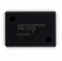
Manufacturer Part Number
DF2328BVF25V
Description
IC H8S MCU FLASH 256K 128QFP
Manufacturer
Renesas Electronics America
Series
H8® H8S/2300r
Datasheets
1.HEWH8E10A.pdf
(19 pages)
2.D12312SVTE25V.pdf
(341 pages)
3.D12322RVF25V.pdf
(1304 pages)
Specifications of DF2328BVF25V
Core Processor
H8S/2000
Core Size
16-Bit
Speed
25MHz
Connectivity
SCI, SmartCard
Peripherals
DMA, POR, PWM, WDT
Number Of I /o
87
Program Memory Size
256KB (256K x 8)
Program Memory Type
FLASH
Ram Size
8K x 8
Voltage - Supply (vcc/vdd)
2.7 V ~ 3.6 V
Data Converters
A/D 8x10b; D/A 2x8b
Oscillator Type
Internal
Operating Temperature
-20°C ~ 75°C
Package / Case
128-QFP
For Use With
EDK2329 - DEV EVALUATION KIT H8S/2329
Lead Free Status / RoHS Status
Lead free / RoHS Compliant
Eeprom Size
-
Other names
HD64F2328BVF25V
Available stocks
Company
Part Number
Manufacturer
Quantity
Price
Company:

Part Number:
DF2328BVF25V
Manufacturer:
Renesas Electronics America
Quantity:
10 000


19.7
In the on-board programming modes, flash memory programming and erasing is performed by
software, using the CPU. There are four flash memory operating modes: program mode, erase
mode, program-verify mode, and erase-verify mode. Transitions to these modes can be made by
setting the PSU, ESU, P, E, PV, and EV bits in FLMCR1.
The flash memory cannot be read while being programmed or erased. Therefore, the program that
controls flash memory programming/erasing (the programming control program) should be
located and executed in on-chip RAM or external memory. When the program is located in
external memory, an instruction for programming the flash memory and the following instruction
should be located in on-chip RAM. The DMAC or DTC should not be activated before or after the
instruction for programming the flash memory is executed.
Notes: 1. Operation is not guaranteed if setting/resetting of the SWE, ESU, PSU, EV, PV, E, and
19.7.1
Follow the procedure shown in the program/program-verify flowchart in figure 19.14 to write data
or programs to flash memory. Performing program operations according to this flowchart will
enable data or programs to be written to flash memory without subjecting the device to voltage
stress or sacrificing program data reliability. Programming should be carried out 128 bytes at a
time.
For the wait times (x, y, z1, z2, z3 α, ß, γ, ε, η, and θ) after bits are set or cleared in flash memory
control register 1 (FLMCR1) and the maximum number of programming operations (N), see
section 22.2.6, Flash Memory Characteristics.
Following the elapse of (x) µs or more after the SWE bit is set to 1 in flash memory control
register 1 (FLMCR1), 128-byte program data is stored in the program data area and reprogram
data area, and the 128-byte data in the reprogram data area is written consecutively to the write
addresses. The lower 8 bits of the first address written to must be H'00 or H'80. 128 consecutive
byte data transfers are performed. The program address and program data are latched in the flash
memory. A 128-byte data transfer must be performed even if writing fewer than 128 bytes; in this
case, H'FF data must be written to the extra addresses.
Next, the watchdog timer is set to prevent overprogramming in the event of program runaway, etc.
Set a value greater than (y + z2 + α + β) µs as the WDT overflow period. After this, preparation
for program mode (program setup) is carried out by setting the PSU bit in FLMCR1, and after the
2. Perform programming in the erased state. Do not perform additional programming on
Programming/Erasing Flash Memory
Program Mode
P bits in FLMCR1 is executed by a program in flash memory.
previously programmed addresses.
Rev.6.00 Sep. 27, 2007 Page 765 of 1268
REJ09B0220-0600
Section 19 ROM
Related parts for DF2328BVF25V
Image
Part Number
Description
Manufacturer
Datasheet
Request
R

Part Number:
Description:
KIT STARTER FOR M16C/29
Manufacturer:
Renesas Electronics America
Datasheet:

Part Number:
Description:
KIT STARTER FOR R8C/2D
Manufacturer:
Renesas Electronics America
Datasheet:

Part Number:
Description:
R0K33062P STARTER KIT
Manufacturer:
Renesas Electronics America
Datasheet:

Part Number:
Description:
KIT STARTER FOR R8C/23 E8A
Manufacturer:
Renesas Electronics America
Datasheet:

Part Number:
Description:
KIT STARTER FOR R8C/25
Manufacturer:
Renesas Electronics America
Datasheet:

Part Number:
Description:
KIT STARTER H8S2456 SHARPE DSPLY
Manufacturer:
Renesas Electronics America
Datasheet:

Part Number:
Description:
KIT STARTER FOR R8C38C
Manufacturer:
Renesas Electronics America
Datasheet:

Part Number:
Description:
KIT STARTER FOR R8C35C
Manufacturer:
Renesas Electronics America
Datasheet:

Part Number:
Description:
KIT STARTER FOR R8CL3AC+LCD APPS
Manufacturer:
Renesas Electronics America
Datasheet:
Part Number:
Description:
KIT STARTER FOR RX610
Manufacturer:
Renesas Electronics America
Datasheet:

Part Number:
Description:
KIT STARTER FOR R32C/118
Manufacturer:
Renesas Electronics America
Datasheet:

Part Number:
Description:
KIT DEV RSK-R8C/26-29
Manufacturer:
Renesas Electronics America
Datasheet:

Part Number:
Description:
KIT STARTER FOR SH7124
Manufacturer:
Renesas Electronics America
Datasheet:

Part Number:
Description:
KIT STARTER FOR H8SX/1622
Manufacturer:
Renesas Electronics America
Datasheet:

Part Number:
Description:
KIT DEV FOR SH7203
Manufacturer:
Renesas Electronics America
Datasheet: