DF2328BVF25V Renesas Electronics America, DF2328BVF25V Datasheet - Page 16
DF2328BVF25V
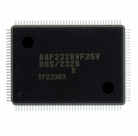
Manufacturer Part Number
DF2328BVF25V
Description
IC H8S MCU FLASH 256K 128QFP
Manufacturer
Renesas Electronics America
Series
H8® H8S/2300r
Datasheets
1.HEWH8E10A.pdf
(19 pages)
2.D12312SVTE25V.pdf
(341 pages)
3.D12322RVF25V.pdf
(1304 pages)
Specifications of DF2328BVF25V
Core Processor
H8S/2000
Core Size
16-Bit
Speed
25MHz
Connectivity
SCI, SmartCard
Peripherals
DMA, POR, PWM, WDT
Number Of I /o
87
Program Memory Size
256KB (256K x 8)
Program Memory Type
FLASH
Ram Size
8K x 8
Voltage - Supply (vcc/vdd)
2.7 V ~ 3.6 V
Data Converters
A/D 8x10b; D/A 2x8b
Oscillator Type
Internal
Operating Temperature
-20°C ~ 75°C
Package / Case
128-QFP
For Use With
EDK2329 - DEV EVALUATION KIT H8S/2329
Lead Free Status / RoHS Status
Lead free / RoHS Compliant
Eeprom Size
-
Other names
HD64F2328BVF25V
Available stocks
Company
Part Number
Manufacturer
Quantity
Price
Company:

Part Number:
DF2328BVF25V
Manufacturer:
Renesas Electronics America
Quantity:
10 000


5.6
Section 6 Bus Controller....................................................................................143
6.1
6.2
6.3
6.4
6.5
Rev.6.00 Sep. 27, 2007 Page xiv of xxx
REJ09B0220-0600
DTC and DMAC Activation by Interrupt ......................................................................... 139
5.6.1
5.6.2
5.6.3
Overview........................................................................................................................... 143
6.1.1
6.1.2
6.1.3
6.1.4
Register Descriptions ........................................................................................................ 149
6.2.1
6.2.2
6.2.3
6.2.4
6.2.5
6.2.6
6.2.7
6.2.8
6.2.9
Overview of Bus Control .................................................................................................. 165
6.3.1
6.3.2
6.3.3
6.3.4
6.3.5
Basic Bus Interface ........................................................................................................... 170
6.4.1
6.4.2
6.4.3
6.4.4
6.4.5
DRAM Interface (Not supported in the H8S/2321) .......................................................... 183
6.5.1
6.5.2
6.5.3
6.5.4
6.5.5
6.5.6
Overview.............................................................................................................. 139
Block Diagram ..................................................................................................... 140
Operation ............................................................................................................. 141
Features................................................................................................................ 143
Block Diagram ..................................................................................................... 145
Pin Configuration................................................................................................. 146
Register Configuration......................................................................................... 148
Bus Width Control Register (ABWCR)............................................................... 149
Access State Control Register (ASTCR) ............................................................. 150
Wait Control Registers H and L (WCRH, WCRL).............................................. 151
Bus Control Register H (BCRH) ......................................................................... 154
Bus Control Register L (BCRL) .......................................................................... 157
Memory Control Register (MCR)........................................................................ 159
DRAM Control Register (DRAMCR) ................................................................. 162
Refresh Timer Counter (RTCNT)........................................................................ 164
Refresh Time Constant Register (RTCOR) ......................................................... 164
Area Partitioning.................................................................................................. 165
Bus Specifications................................................................................................ 166
Memory Interfaces ............................................................................................... 167
Advanced Mode ................................................................................................... 168
Chip Select Signals .............................................................................................. 169
Overview.............................................................................................................. 170
Data Size and Data Alignment............................................................................. 170
Valid Strobes........................................................................................................ 172
Basic Timing........................................................................................................ 173
Wait Control ........................................................................................................ 181
Overview.............................................................................................................. 183
Setting DRAM Space........................................................................................... 183
Address Multiplexing........................................................................................... 184
Data Bus............................................................................................................... 184
Pins Used for DRAM Interface............................................................................ 185
Basic Timing........................................................................................................ 186
Related parts for DF2328BVF25V
Image
Part Number
Description
Manufacturer
Datasheet
Request
R

Part Number:
Description:
KIT STARTER FOR M16C/29
Manufacturer:
Renesas Electronics America
Datasheet:

Part Number:
Description:
KIT STARTER FOR R8C/2D
Manufacturer:
Renesas Electronics America
Datasheet:

Part Number:
Description:
R0K33062P STARTER KIT
Manufacturer:
Renesas Electronics America
Datasheet:

Part Number:
Description:
KIT STARTER FOR R8C/23 E8A
Manufacturer:
Renesas Electronics America
Datasheet:

Part Number:
Description:
KIT STARTER FOR R8C/25
Manufacturer:
Renesas Electronics America
Datasheet:

Part Number:
Description:
KIT STARTER H8S2456 SHARPE DSPLY
Manufacturer:
Renesas Electronics America
Datasheet:

Part Number:
Description:
KIT STARTER FOR R8C38C
Manufacturer:
Renesas Electronics America
Datasheet:

Part Number:
Description:
KIT STARTER FOR R8C35C
Manufacturer:
Renesas Electronics America
Datasheet:

Part Number:
Description:
KIT STARTER FOR R8CL3AC+LCD APPS
Manufacturer:
Renesas Electronics America
Datasheet:
Part Number:
Description:
KIT STARTER FOR RX610
Manufacturer:
Renesas Electronics America
Datasheet:

Part Number:
Description:
KIT STARTER FOR R32C/118
Manufacturer:
Renesas Electronics America
Datasheet:

Part Number:
Description:
KIT DEV RSK-R8C/26-29
Manufacturer:
Renesas Electronics America
Datasheet:

Part Number:
Description:
KIT STARTER FOR SH7124
Manufacturer:
Renesas Electronics America
Datasheet:

Part Number:
Description:
KIT STARTER FOR H8SX/1622
Manufacturer:
Renesas Electronics America
Datasheet:

Part Number:
Description:
KIT DEV FOR SH7203
Manufacturer:
Renesas Electronics America
Datasheet: