DF2328BVF25V Renesas Electronics America, DF2328BVF25V Datasheet - Page 471
DF2328BVF25V
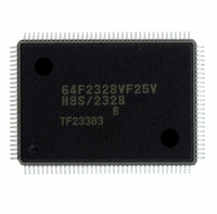
Manufacturer Part Number
DF2328BVF25V
Description
IC H8S MCU FLASH 256K 128QFP
Manufacturer
Renesas Electronics America
Series
H8® H8S/2300r
Datasheets
1.HEWH8E10A.pdf
(19 pages)
2.D12312SVTE25V.pdf
(341 pages)
3.D12322RVF25V.pdf
(1304 pages)
Specifications of DF2328BVF25V
Core Processor
H8S/2000
Core Size
16-Bit
Speed
25MHz
Connectivity
SCI, SmartCard
Peripherals
DMA, POR, PWM, WDT
Number Of I /o
87
Program Memory Size
256KB (256K x 8)
Program Memory Type
FLASH
Ram Size
8K x 8
Voltage - Supply (vcc/vdd)
2.7 V ~ 3.6 V
Data Converters
A/D 8x10b; D/A 2x8b
Oscillator Type
Internal
Operating Temperature
-20°C ~ 75°C
Package / Case
128-QFP
For Use With
EDK2329 - DEV EVALUATION KIT H8S/2329
Lead Free Status / RoHS Status
Lead free / RoHS Compliant
Eeprom Size
-
Other names
HD64F2328BVF25V
Available stocks
Company
Part Number
Manufacturer
Quantity
Price
Company:

Part Number:
DF2328BVF25V
Manufacturer:
Renesas Electronics America
Quantity:
10 000


9.14.3
Port G pins also function as bus control signal output pins (CS
functions are different in mode 7, and modes 4 to 6. Port G pin functions are shown in table 9.27.
Note: * The CAS is not supported in the H8S/2321.
Table 9.27 Port G Pin Functions
Pin
PG
PG
PG
4
3
2
/CS
/CS
/CS
0
1
2
Pin Functions
The pin function is switched as shown below according to the operating mode
and bit PG4DDR.
The pin function is switched as shown below according to the operating mode
and bits PG3DDR and CS167E.
The pin function is switched as shown below according to the operating mode
and bits PG2DDR and CS25E.
Selection Method and Pin Functions
Operating
Mode
PG4DDR
Pin function
Operating
Mode
PG3DDR
CS167E
Pin function
Operating
Mode
PG2DDR
CS25E
Pin function
PG
PG
PG
4
3
2
pin
pin
—
—
0
0
input pin CS
input
input
0
Modes 4 to 6
Modes 4 to 6
Modes 4 to 6
PG
PG
3
2
pin
pin
output
output
0
0
0
Rev.6.00 Sep. 27, 2007 Page 439 of 1268
output pin PG
1
1
1
CS
CS
0
to CS
1
2
pin
pin
output
output
1
1
3
, and CAS * ). The pin
4
input pin PG
0
PG
PG
3
pin
2
pin
Section 9 I/O Ports
—
—
Mode 7
0
0
input
input
REJ09B0220-0600
Mode 7
Mode 7
4
PG
PG
output pin
1
3
2
pin
pin
—
—
output
output
1
1
Related parts for DF2328BVF25V
Image
Part Number
Description
Manufacturer
Datasheet
Request
R

Part Number:
Description:
KIT STARTER FOR M16C/29
Manufacturer:
Renesas Electronics America
Datasheet:

Part Number:
Description:
KIT STARTER FOR R8C/2D
Manufacturer:
Renesas Electronics America
Datasheet:

Part Number:
Description:
R0K33062P STARTER KIT
Manufacturer:
Renesas Electronics America
Datasheet:

Part Number:
Description:
KIT STARTER FOR R8C/23 E8A
Manufacturer:
Renesas Electronics America
Datasheet:

Part Number:
Description:
KIT STARTER FOR R8C/25
Manufacturer:
Renesas Electronics America
Datasheet:

Part Number:
Description:
KIT STARTER H8S2456 SHARPE DSPLY
Manufacturer:
Renesas Electronics America
Datasheet:

Part Number:
Description:
KIT STARTER FOR R8C38C
Manufacturer:
Renesas Electronics America
Datasheet:

Part Number:
Description:
KIT STARTER FOR R8C35C
Manufacturer:
Renesas Electronics America
Datasheet:

Part Number:
Description:
KIT STARTER FOR R8CL3AC+LCD APPS
Manufacturer:
Renesas Electronics America
Datasheet:
Part Number:
Description:
KIT STARTER FOR RX610
Manufacturer:
Renesas Electronics America
Datasheet:

Part Number:
Description:
KIT STARTER FOR R32C/118
Manufacturer:
Renesas Electronics America
Datasheet:

Part Number:
Description:
KIT DEV RSK-R8C/26-29
Manufacturer:
Renesas Electronics America
Datasheet:

Part Number:
Description:
KIT STARTER FOR SH7124
Manufacturer:
Renesas Electronics America
Datasheet:

Part Number:
Description:
KIT STARTER FOR H8SX/1622
Manufacturer:
Renesas Electronics America
Datasheet:

Part Number:
Description:
KIT DEV FOR SH7203
Manufacturer:
Renesas Electronics America
Datasheet: