DK-DEV-3SL150N Altera, DK-DEV-3SL150N Datasheet - Page 12
DK-DEV-3SL150N
Manufacturer Part Number
DK-DEV-3SL150N
Description
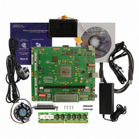
KIT DEVELOPMENT STRATIX III
Manufacturer
Altera
Series
Stratix® IIIr
Type
FPGAr
Datasheets
1.EP3SL150F780C4N.pdf
(16 pages)
2.EP3SL150F780C4N.pdf
(332 pages)
3.DK-DEV-3SL150N.pdf
(34 pages)
Specifications of DK-DEV-3SL150N
Contents
Development Platform, Cables and Software
Silicon Manufacturer
Altera
Core Architecture
FPGA
Core Sub-architecture
Stratix
Silicon Core Number
EP3S
Silicon Family Name
Stratix III
Kit Contents
Development Board, Cable And Accessories
Rohs Compliant
Yes
For Use With/related Products
EP3SL150F152
Lead Free Status / RoHS Status
Lead free / RoHS Compliant
Other names
544-2568
Available stocks
Company
Part Number
Manufacturer
Quantity
Price
Company:

Part Number:
DK-DEV-3SL150N
Manufacturer:
Altera
Quantity:
135


1–12
Table 1–18. Differential I/O Standard Specifications (Part 2 of 2)
Power Consumption
Stratix III Device Handbook, Volume 2
2.5 V LVDS
(Column I/O)
RSDS
(Row I/O)
RSDS
(Column I/O)
Mini-LVDS
(Row I/O)
Mini-LVDS
(Column I/0)
LVPECL
(3)
Notes to
(1) The minimum V
(2) RL range: 90 RL 110 .
(3) Column and row I/O banks support LVPECL I/O standards for input operation only on dedicated clock input pins. Differential clock inputs in column I/O use
(4) The receiver voltage input range for the data rate when D
(5) Power supply for the column I/O LVPECL differential clock input buffer is V
(6) The receiver voltage input range for the data rate when D
Standard
V
The receiver voltage input range for the data rate when D
The receiver voltage input range for the data rate when D
I/O
CC_CLKIN
Table
that must be powered by 2.5 V. Differential clock inputs in row I/O banks are powered by V
f
1–18:
2.375
2.375
2.375
2.375
2.375
2.375
2.375
2.375
Min
(5)
(5)
ID
value is applicable over the entire common mode range, V
V
CCIO
Typ
2.5
2.5
2.5
2.5
2.5
2.5
2.5
2.5
(5)
(5)
Altera offers two ways to estimate power for a design: the Excel-based Early Power
Estimator (EPE) and the Quartus
The interactive Excel-based Early Power Estimator is typically used prior to designing
the FPGA in order to get a magnitude estimate of the device power. The Quartus II
PowerPlay Power Analyzer provides estimation based on the specifics of the design
after place-and-route is complete. The PowerPlay Power Analyzer can apply a
combination of user-entered, simulation-derived, and estimated signal activities
which, when combined with detailed circuit models, can yield very accurate power
estimation.
Refer to
Use the EPE and PowerPlay Power Analyzer for current estimates of remaining
power supplies.
For more information about power estimation tools, refer to the
Estimator User Guide For Stratix III FPGAs
the Quartus II Handbook.
(V)
2.625
2.625
2.625
2.625
2.625
2.625
2.625
2.625
Max
(5)
(5)
Table 1–4 on page 1–5
Min
0.1
0.1
0.1
0.1
0.2
0.2
0.3
0.3
Condition
V
V
V
V
V
CM
CM
CM
CM
ID
= 1.25
= 1.25
= 1.25
= 1.25
—
—
—
—
(V)
(1)
max
max
max
max
> 700 Mbps is 0.85 V V
700 Mbps is 0.45 V V
> 700 Mbps is 1.0 V V
700 Mbps is zero V V
Max
0.6
0.6
—
—
—
—
—
—
Chapter 1: Stratix III Device Datasheet: DC and Switching Characteristics
for supply current estimates for V
II PowerPlay Power Analyzer feature.
0.05
Min
1.05
0.3
0.3
0.4
0.4
0.6
1.0
(6)
(6)
CC_CLKIN
CM
.
Condition
and the
D
D
D
D
.
V
max
max
max
max
ICM(DC)
Mbps
Mbps
Mbps
Mbps
IN
700
—
—
—
—
700
> 700
> 700
IN
IN
IN
1.6 V.
1.75 V.
1.85 V.
1.95 V.
(V)
PowerPlay Power Analysis
1.325
1.325
Max
1.55
1.4
1.4
1.8
(4)
1.6
(4)
1.8
(6)
(6)
CCPD
.
0.247
0.247
0.25
0.25
Min
0.1
0.1
—
—
© July 2010 Altera Corporation
PowerPlay Early Power
V
CCPGM
OD
Typ
0.2
0.2
—
—
—
—
—
—
(V)
Electrical Characteristics
and V
(2)
Max
0.6
0.6
0.6
0.6
0.6
0.6
—
—
chapter in
CC_CLKIN
Min
1.0
1.0
0.5
0.5
0.5
0.5
—
—
.
V
OCM
1.25
1.25
Typ
1.2
1.2
1.2
1.2
(V)
—
—
(2)
Max
1.5
1.5
1.4
1.5
1.4
1.5
—
—
Related parts for DK-DEV-3SL150N
Image
Part Number
Description
Manufacturer
Datasheet
Request
R

Part Number:
Description:
KIT DEV ARRIA II GX FPGA 2AGX125
Manufacturer:
Altera
Datasheet:

Part Number:
Description:
KIT DEV CYCLONE III LS EP3CLS200
Manufacturer:
Altera
Datasheet:

Part Number:
Description:
KIT DEV STRATIX IV FPGA 4SE530
Manufacturer:
Altera
Datasheet:

Part Number:
Description:
KIT DEV FPGA 2AGX260 W/6.375G TX
Manufacturer:
Altera
Datasheet:

Part Number:
Description:
KIT DEV MAX V 5M570Z
Manufacturer:
Altera
Datasheet:

Part Number:
Description:
KIT DEV STRATIX V FPGA 5SGXEA7
Manufacturer:
Altera
Datasheet:

Part Number:
Description:
KIT DEVELOPMENT STRATIX IV
Manufacturer:
Altera
Datasheet:

Part Number:
Description:
KIT DEV ARRIA GX 1AGX60N
Manufacturer:
Altera
Datasheet:
Part Number:
Description:
KIT STARTER CYCLONE IV GX
Manufacturer:
Altera
Datasheet:
Part Number:
Description:
KIT DEVELOPMENT STRATIX IV
Manufacturer:
Altera
Datasheet:

Part Number:
Description:
CPLD, EP610 Family, ECMOS Process, 300 Gates, 16 Macro Cells, 16 Reg., 16 User I/Os, 5V Supply, 35 Speed Grade, 24DIP
Manufacturer:
Altera Corporation
Datasheet:
Part Number:
Description:
CPLD, EP610 Family, ECMOS Process, 300 Gates, 16 Macro Cells, 16 Reg., 16 User I/Os, 5V Supply, 15 Speed Grade, 24DIP
Manufacturer:
Altera Corporation
Datasheet: