DK-DEV-3SL150N Altera, DK-DEV-3SL150N Datasheet - Page 2
DK-DEV-3SL150N
Manufacturer Part Number
DK-DEV-3SL150N
Description
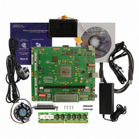
KIT DEVELOPMENT STRATIX III
Manufacturer
Altera
Series
Stratix® IIIr
Type
FPGAr
Datasheets
1.EP3SL150F780C4N.pdf
(16 pages)
2.EP3SL150F780C4N.pdf
(332 pages)
3.DK-DEV-3SL150N.pdf
(34 pages)
Specifications of DK-DEV-3SL150N
Contents
Development Platform, Cables and Software
Silicon Manufacturer
Altera
Core Architecture
FPGA
Core Sub-architecture
Stratix
Silicon Core Number
EP3S
Silicon Family Name
Stratix III
Kit Contents
Development Board, Cable And Accessories
Rohs Compliant
Yes
For Use With/related Products
EP3SL150F152
Lead Free Status / RoHS Status
Lead free / RoHS Compliant
Other names
544-2568
Available stocks
Company
Part Number
Manufacturer
Quantity
Price
Company:

Part Number:
DK-DEV-3SL150N
Manufacturer:
Altera
Quantity:
135


1–2
Table 1–1. Absolute Maximum Ratings for Stratix III Devices
Stratix III Device Handbook, Volume 2
V
V
V
T
I
T
Note to
(1) Supply voltage specifications apply to voltage readings taken at the device pins, not the power supply.
OUT
J
STG
CC_CLKIN
CCBAT
I
Symbol
Table
1–1:
1
Sinusoidal Maximum Allowed Overshoot/Undershoot Voltage
During transitions, input signals may overshoot to the voltage listed in
undershoot to –2.0 V for input currents less than 100 mA and periods shorter than
20 ns.
Table 1–2
overshoot voltage as a percentage over the lifetime of the device. The maximum
allowed overshoot duration is specified as percentage of high-time over the lifetime of
the device.
A DC signal is equivalent to 100% duty cycle. For example, a signal that overshoots to
4.2 V can only be at 4.2 V for 15.8% over the lifetime of the device; for a device lifetime
of 10 years, this is equivalent to 15.8% of ten years which is 18.96 months.
shows how to determine the overshoot duration.
Figure 1–1. Overshoot Duration
In the example shown in
present at the Stratix III pin, up to 4.1 V. From
V, the percentage of high time for overshoot > 3.15 V can be as high as 46% over an
11.4-year period. The percentage of high time is calculated as (delta T/T) * 100. This
11.4-year period assumes the device is always turned on with 100% I/O toggle rate
and 50% duty cycle signal. For lower I/O toggle rates and situations where the device
is in an idle state, lifetimes are increased.
Differential clock input power supply (top and bottom I/O
banks only)
Battery back-up power supply for design security volatile
key register
DC Input voltage
Operating junction temperature
DC output current, per pin
Storage temperature (No bias)
lists the maximum allowed input overshoot voltage and the duration of the
Parameter
4.1 V
3.15 V
3.0 V
Figure
Chapter 1: Stratix III Device Datasheet: DC and Switching Characteristics
1–1, the overshoot voltage is shown in red and is
(Note 1)
ΔT
(Part 2 of 2)
T
Table
1–2, for an overshoot of up to 4.1
Minimum
-0.5
-0.5
-0.5
-55
-25
-65
© July 2010 Altera Corporation
Maximum
Electrical Characteristics
3.75
3.75
125
150
4.0
40
Table 1–2
Figure 1–1
Unit
mA
°C
°C
V
V
V
and
Related parts for DK-DEV-3SL150N
Image
Part Number
Description
Manufacturer
Datasheet
Request
R

Part Number:
Description:
KIT DEV ARRIA II GX FPGA 2AGX125
Manufacturer:
Altera
Datasheet:

Part Number:
Description:
KIT DEV CYCLONE III LS EP3CLS200
Manufacturer:
Altera
Datasheet:

Part Number:
Description:
KIT DEV STRATIX IV FPGA 4SE530
Manufacturer:
Altera
Datasheet:

Part Number:
Description:
KIT DEV FPGA 2AGX260 W/6.375G TX
Manufacturer:
Altera
Datasheet:

Part Number:
Description:
KIT DEV MAX V 5M570Z
Manufacturer:
Altera
Datasheet:

Part Number:
Description:
KIT DEV STRATIX V FPGA 5SGXEA7
Manufacturer:
Altera
Datasheet:

Part Number:
Description:
KIT DEVELOPMENT STRATIX IV
Manufacturer:
Altera
Datasheet:

Part Number:
Description:
KIT DEV ARRIA GX 1AGX60N
Manufacturer:
Altera
Datasheet:
Part Number:
Description:
KIT STARTER CYCLONE IV GX
Manufacturer:
Altera
Datasheet:
Part Number:
Description:
KIT DEVELOPMENT STRATIX IV
Manufacturer:
Altera
Datasheet:

Part Number:
Description:
CPLD, EP610 Family, ECMOS Process, 300 Gates, 16 Macro Cells, 16 Reg., 16 User I/Os, 5V Supply, 35 Speed Grade, 24DIP
Manufacturer:
Altera Corporation
Datasheet:
Part Number:
Description:
CPLD, EP610 Family, ECMOS Process, 300 Gates, 16 Macro Cells, 16 Reg., 16 User I/Os, 5V Supply, 15 Speed Grade, 24DIP
Manufacturer:
Altera Corporation
Datasheet: