DK-DEV-3SL150N Altera, DK-DEV-3SL150N Datasheet - Page 30
DK-DEV-3SL150N
Manufacturer Part Number
DK-DEV-3SL150N
Description
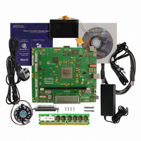
KIT DEVELOPMENT STRATIX III
Manufacturer
Altera
Series
Stratix® IIIr
Type
FPGAr
Datasheets
1.EP3SL150F780C4N.pdf
(16 pages)
2.EP3SL150F780C4N.pdf
(332 pages)
3.DK-DEV-3SL150N.pdf
(34 pages)
Specifications of DK-DEV-3SL150N
Contents
Development Platform, Cables and Software
Silicon Manufacturer
Altera
Core Architecture
FPGA
Core Sub-architecture
Stratix
Silicon Core Number
EP3S
Silicon Family Name
Stratix III
Kit Contents
Development Board, Cable And Accessories
Rohs Compliant
Yes
For Use With/related Products
EP3SL150F152
Lead Free Status / RoHS Status
Lead free / RoHS Compliant
Other names
544-2568
Available stocks
Company
Part Number
Manufacturer
Quantity
Price
Company:

Part Number:
DK-DEV-3SL150N
Manufacturer:
Altera
Quantity:
135


1–30
Table 1–34. On-Chip Termination Calibration Block Specification
I/O Timing
Timing Model
Stratix III Device Handbook, Volume 2
OCTUSRCLK
t
t
t
OCTCAL
OCTSHIFT
RS_RT
Symbol
Clock required by OCT calibration blocks
Number of OCTUSRCLK clock cycles required
for OCT Rs and Rt calibration
Number of OCTUSRCLK clock cycles required
for OCT code to shift out per OCT calibration block
Time required to dynamically switch from Rs to Rt
OCT Calibration Block Specifications
Table 1–34
devices.
DCD Specifications
Table 1–35
Table 1–35. Duty Cycle Distortion on Stratix III I/O Pins
The following sections describe the timing models, preliminary and final timings, I/O
timing measurement methodology, I/O default capacitive loading, programmable
IOE delay, programmable output buffer delay, user I/O timing, and dedicated clock
pin timing.
The DirectDrive technology and MultiTrack interconnect ensure predictable
performance, accurate simulation, and accurate timing analysis across all Stratix III
device densities and speed grades. This section describes the performance of the
Stratix III device I/Os.
All specifications except the fast model are representative of worst-case supply
voltage and junction temperature conditions. Fast model specifications are
representative of best case process, supply voltage, and junction temperature
conditions.
The timing numbers listed in this section are extracted from the Quartus II software
version 8.1.
Output Duty Cycle
Note to
(1) The DCD specification applies to clock outputs from the PLLs, global clock tree, and IOE driving dedicated and
general-purpose I/O pins.
Table
lists the on-chip termination calibration block specifications for Stratix III
lists the worst case duty cycle distortion for Stratix III devices.
1–35:
Symbol
Description
Chapter 1: Stratix III Device Datasheet: DC and Switching Characteristics
Min
45
C2
Max
55
(Note 1)
Min
45
C3
Min
Max
—
—
—
—
55
© July 2010 Altera Corporation
Typical
Min
1000
45
2.5
—
28
C4
Max
55
Max
20
—
—
—
I/O Timing
cycles
cycles
Unit
MHz
Unit
%
ns
Related parts for DK-DEV-3SL150N
Image
Part Number
Description
Manufacturer
Datasheet
Request
R

Part Number:
Description:
KIT DEV ARRIA II GX FPGA 2AGX125
Manufacturer:
Altera
Datasheet:

Part Number:
Description:
KIT DEV CYCLONE III LS EP3CLS200
Manufacturer:
Altera
Datasheet:

Part Number:
Description:
KIT DEV STRATIX IV FPGA 4SE530
Manufacturer:
Altera
Datasheet:

Part Number:
Description:
KIT DEV FPGA 2AGX260 W/6.375G TX
Manufacturer:
Altera
Datasheet:

Part Number:
Description:
KIT DEV MAX V 5M570Z
Manufacturer:
Altera
Datasheet:

Part Number:
Description:
KIT DEV STRATIX V FPGA 5SGXEA7
Manufacturer:
Altera
Datasheet:

Part Number:
Description:
KIT DEVELOPMENT STRATIX IV
Manufacturer:
Altera
Datasheet:

Part Number:
Description:
KIT DEV ARRIA GX 1AGX60N
Manufacturer:
Altera
Datasheet:
Part Number:
Description:
KIT STARTER CYCLONE IV GX
Manufacturer:
Altera
Datasheet:
Part Number:
Description:
KIT DEVELOPMENT STRATIX IV
Manufacturer:
Altera
Datasheet:

Part Number:
Description:
CPLD, EP610 Family, ECMOS Process, 300 Gates, 16 Macro Cells, 16 Reg., 16 User I/Os, 5V Supply, 35 Speed Grade, 24DIP
Manufacturer:
Altera Corporation
Datasheet:
Part Number:
Description:
CPLD, EP610 Family, ECMOS Process, 300 Gates, 16 Macro Cells, 16 Reg., 16 User I/Os, 5V Supply, 15 Speed Grade, 24DIP
Manufacturer:
Altera Corporation
Datasheet: