DK-DEV-3SL150N Altera, DK-DEV-3SL150N Datasheet - Page 31
DK-DEV-3SL150N
Manufacturer Part Number
DK-DEV-3SL150N
Description
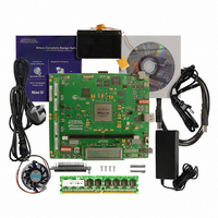
KIT DEVELOPMENT STRATIX III
Manufacturer
Altera
Series
Stratix® IIIr
Type
FPGAr
Datasheets
1.EP3SL150F780C4N.pdf
(16 pages)
2.EP3SL150F780C4N.pdf
(332 pages)
3.DK-DEV-3SL150N.pdf
(34 pages)
Specifications of DK-DEV-3SL150N
Contents
Development Platform, Cables and Software
Silicon Manufacturer
Altera
Core Architecture
FPGA
Core Sub-architecture
Stratix
Silicon Core Number
EP3S
Silicon Family Name
Stratix III
Kit Contents
Development Board, Cable And Accessories
Rohs Compliant
Yes
For Use With/related Products
EP3SL150F152
Lead Free Status / RoHS Status
Lead free / RoHS Compliant
Other names
544-2568
Available stocks
Company
Part Number
Manufacturer
Quantity
Price
Company:

Part Number:
DK-DEV-3SL150N
Manufacturer:
Altera
Quantity:
135


Chapter 1: Stratix III Device Datasheet: DC and Switching Characteristics
I/O Timing
Preliminary and Final Timing
I/O Timing Measurement Methodology
© July 2010 Altera Corporation
Timing models can have either preliminary or final status. The Quartus II software
issues an informational message during design compilation if the timing models are
preliminary.
Preliminary status means that the timing models are subject to change in future
Quartus II releases. Initially, timing numbers are created using simulation results,
process data, and other known parameters. Parts of the timing models may be
correlated to silicon measurements. Various tests are used to make the preliminary
numbers as close to the actual timing parameters as possible.
Final timing models are based on simulation models that are characterized versus the
actual device measurements under all allowable operating conditions. When the
timing models are final, all or most of the Stratix III family devices have been
completely characterized and no further changes to the timing model are expected.
Table 1–36. Timing Model Status for Stratix III Devices
Altera characterizes timing delays at the worst-case process, minimum voltage, and
maximum temperature for input register setup time (t
Quartus II software uses the following equations to calculate t
Stratix III devices input signals.
t
+ data delay from the input pin to the input register
+ micro setup time of the input register
- clock delay from the input pin to the input register
t
- data delay from the input pin to the input register
+ micro hold time of the input register
+ clock delay from the input pin to the input register
su
h
EP3SL50
EP3SL70
EP3SL110
EP3SL150
EP3SL200
EP3SL340
EP3SE50
EP3SE80
EP3SE110
EP3SE260
=
=
Table 1–36
Device
lists the status of the Stratix III device timing models.
Preliminary
—
—
—
—
—
—
—
—
—
—
su
) and hold time (t
Stratix III Device Handbook, Volume 2
su
and t
h
timing for the
h
Final
). The
v
v
v
v
v
v
v
v
v
v
1–31
Related parts for DK-DEV-3SL150N
Image
Part Number
Description
Manufacturer
Datasheet
Request
R

Part Number:
Description:
KIT DEV ARRIA II GX FPGA 2AGX125
Manufacturer:
Altera
Datasheet:

Part Number:
Description:
KIT DEV CYCLONE III LS EP3CLS200
Manufacturer:
Altera
Datasheet:

Part Number:
Description:
KIT DEV STRATIX IV FPGA 4SE530
Manufacturer:
Altera
Datasheet:

Part Number:
Description:
KIT DEV FPGA 2AGX260 W/6.375G TX
Manufacturer:
Altera
Datasheet:

Part Number:
Description:
KIT DEV MAX V 5M570Z
Manufacturer:
Altera
Datasheet:

Part Number:
Description:
KIT DEV STRATIX V FPGA 5SGXEA7
Manufacturer:
Altera
Datasheet:

Part Number:
Description:
KIT DEVELOPMENT STRATIX IV
Manufacturer:
Altera
Datasheet:

Part Number:
Description:
KIT DEV ARRIA GX 1AGX60N
Manufacturer:
Altera
Datasheet:
Part Number:
Description:
KIT STARTER CYCLONE IV GX
Manufacturer:
Altera
Datasheet:
Part Number:
Description:
KIT DEVELOPMENT STRATIX IV
Manufacturer:
Altera
Datasheet:

Part Number:
Description:
CPLD, EP610 Family, ECMOS Process, 300 Gates, 16 Macro Cells, 16 Reg., 16 User I/Os, 5V Supply, 35 Speed Grade, 24DIP
Manufacturer:
Altera Corporation
Datasheet:
Part Number:
Description:
CPLD, EP610 Family, ECMOS Process, 300 Gates, 16 Macro Cells, 16 Reg., 16 User I/Os, 5V Supply, 15 Speed Grade, 24DIP
Manufacturer:
Altera Corporation
Datasheet: