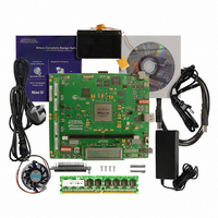
DK-DEV-3SL150N Altera, DK-DEV-3SL150N Datasheet - Page 8

DK-DEV-3SL150N
Manufacturer Part Number
DK-DEV-3SL150N
Description
KIT DEVELOPMENT STRATIX III
Manufacturer
Altera
Series
Stratix® IIIr
Type
FPGAr
Datasheets
1.EP3SL150F780C4N.pdf
(16 pages)
2.EP3SL150F780C4N.pdf
(332 pages)
3.DK-DEV-3SL150N.pdf
(34 pages)
Specifications of DK-DEV-3SL150N
Contents
Development Platform, Cables and Software
Silicon Manufacturer
Altera
Core Architecture
FPGA
Core Sub-architecture
Stratix
Silicon Core Number
EP3S
Silicon Family Name
Stratix III
Kit Contents
Development Board, Cable And Accessories
Rohs Compliant
Yes
For Use With/related Products
EP3SL150F152
Lead Free Status / RoHS Status
Lead free / RoHS Compliant
Other names
544-2568
Available stocks
Company
Part Number
Manufacturer
Quantity
Price
Company:
Part Number:
DK-DEV-3SL150N
Manufacturer:
Altera
Quantity:
135
- Current page: 8 of 332
- Download datasheet (4Mb)
1–8
Table 1–9. On-Chip Termination Variation after Power-up Calibration
Stratix III Device Handbook, Volume 2
dR/dV
dR/dT
Note to
(1) Valid for V
Symbol
Table
1–9:
CCIO
OCT variation with voltage without re-calibration
OCT variation with temperature without re-calibration
range of ± 5% and temperature range of 0° to 85° C.
Pin Capacitance
Table 1–10
s
Table 1–10. Pin Capacitance for Stratix III Device Family
Hot-Socketing
Table 1–11
Table 1–11. Hot-Socketing Specifications for Stratix III Devices
Note to
(1) The I/O ramp rate is 10 ns or more. For ramp rates faster than 10 ns, |I
C
CLK1
capacitance and dv/dt is the slew rate.
, C
Symbol
Table
CLK3
C
C
C
C
C
C
CLKTB
CLKLR
OUTFB
CLK10
IOTB
IOLR
, C
|I
|I
lists the hot-socketing specifications for Stratix III devices.
lists the Stratix III device family pin capacitance.
Description
Symbol
IOPIN
IOPIN
1–11:
CLK8
|(DC)
|(AC)
, and
Input capacitance on top and bottom I/O pins
Input capacitance on left and right I/O pins
Input capacitance on top and bottom
non-dedicated clock input pins
Input capacitance on left and right
non-dedicated clock input pins
Input capacitance on dual-purpose clock
output and feedback pins
Input capacitance for dedicated clock input
pins
Chapter 1: Stratix III Device Datasheet: DC and Switching Characteristics
DC current per I/O pin
AC current per I/O pin
Parameter
Parameter
(Note 1)
V
CCIO
2.5
1.8
1.5
1.2
2.5
1.8
1.5
1.2
3
3
(V)
IOPIN
| = C dv/dt, in which C is I/O pin
Commercial
Typical
© July 2010 Altera Corporation
0.029
0.036
0.065
0.104
0.177
0.294
0.301
0.355
0.344
0.348
Typical
4
4
4
4
5
2
Maximum
Electrical Characteristics
8 mA
300 A
Unit
pF
pF
pF
pF
pF
pF
(1)
%/mV
%/mV
%/mV
%/mV
%/mV
%/°C
%/°C
%/°C
%/°C
%/°C
Unit
Related parts for DK-DEV-3SL150N
Image
Part Number
Description
Manufacturer
Datasheet
Request
R

Part Number:
Description:
KIT DEV ARRIA II GX FPGA 2AGX125
Manufacturer:
Altera
Datasheet:

Part Number:
Description:
KIT DEV CYCLONE III LS EP3CLS200
Manufacturer:
Altera
Datasheet:

Part Number:
Description:
KIT DEV STRATIX IV FPGA 4SE530
Manufacturer:
Altera
Datasheet:

Part Number:
Description:
KIT DEV FPGA 2AGX260 W/6.375G TX
Manufacturer:
Altera
Datasheet:

Part Number:
Description:
KIT DEV MAX V 5M570Z
Manufacturer:
Altera
Datasheet:

Part Number:
Description:
KIT DEV STRATIX V FPGA 5SGXEA7
Manufacturer:
Altera
Datasheet:

Part Number:
Description:
KIT DEVELOPMENT STRATIX IV
Manufacturer:
Altera
Datasheet:

Part Number:
Description:
KIT DEV ARRIA GX 1AGX60N
Manufacturer:
Altera
Datasheet:

Part Number:
Description:
KIT STARTER CYCLONE IV GX
Manufacturer:
Altera
Datasheet:

Part Number:
Description:
KIT DEVELOPMENT STRATIX IV
Manufacturer:
Altera
Datasheet:

Part Number:
Description:
CPLD, EP610 Family, ECMOS Process, 300 Gates, 16 Macro Cells, 16 Reg., 16 User I/Os, 5V Supply, 35 Speed Grade, 24DIP
Manufacturer:
Altera Corporation
Datasheet:

Part Number:
Description:
CPLD, EP610 Family, ECMOS Process, 300 Gates, 16 Macro Cells, 16 Reg., 16 User I/Os, 5V Supply, 15 Speed Grade, 24DIP
Manufacturer:
Altera Corporation
Datasheet:


