DK-DEV-3SL150N Altera, DK-DEV-3SL150N Datasheet - Page 29
DK-DEV-3SL150N
Manufacturer Part Number
DK-DEV-3SL150N
Description
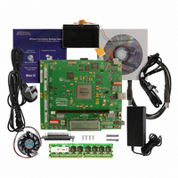
KIT DEVELOPMENT STRATIX III
Manufacturer
Altera
Series
Stratix® IIIr
Type
FPGAr
Datasheets
1.EP3SL150F780C4N.pdf
(16 pages)
2.EP3SL150F780C4N.pdf
(332 pages)
3.DK-DEV-3SL150N.pdf
(34 pages)
Specifications of DK-DEV-3SL150N
Contents
Development Platform, Cables and Software
Silicon Manufacturer
Altera
Core Architecture
FPGA
Core Sub-architecture
Stratix
Silicon Core Number
EP3S
Silicon Family Name
Stratix III
Kit Contents
Development Board, Cable And Accessories
Rohs Compliant
Yes
For Use With/related Products
EP3SL150F152
Lead Free Status / RoHS Status
Lead free / RoHS Compliant
Other names
544-2568
Available stocks
Company
Part Number
Manufacturer
Quantity
Price
Company:

Part Number:
DK-DEV-3SL150N
Manufacturer:
Altera
Quantity:
135


Chapter 1: Stratix III Device Datasheet: DC and Switching Characteristics
Switching Characteristics
Table 1–32. DQS Phase Shift Error Specification for DLL-Delayed Clock (t
Table 1–33. Memory Output Clock Jitter Specification for Stratix III Devices
© July 2010 Altera Corporation
Note to
(1) This error specification is the absolute maximum and minimum error. For example, skew on three DQS delay buffers in a C2 speed grade is
Clock period jitter
Cycle-to-cycle period jitter
Duty cycle jitter
Clock period jitter
Cycle-to-cycle period jitter
Duty cycle jitter
Notes to
(1) The memory output clock jitter measurements are for 200 consecutive clock cycles, as specified in the JEDEC DDR2/DDR3 standard.
(2) The clock jitter specification applies to memory output clock pins generated using differential signal-splitter and DDIO circuits clocked by a PLL output routed
Number of DQS Delay
± 39 ps.
on a regional or global clock network as specified. Altera recommends using the regional clock networks whenever possible.
Table
Parameter
Table
Buffer
1
2
3
4
1–32:
1–33:
Table 1–31
Table 1–31. Average DQS Phase Offset Delay per Setting for Stratix III Devices
Table 1–32
(t
Table 1–33
Notes to
(1) The valid settings for phase offset are -64 to +63 for frequency modes 0 to 3 and -32 to +31 for frequency modes
(2) The typical value equals the average of the minimum and maximum values.
(3) The delay settings are linear with a cumulative delay variation of ± 20 ps for all speed grades. For example, when
DQS_PSERR
Speed Grade
4 to 6.
using a C2 speed grade and applying 10° phase offset settings to a 90° phase shift at 400 MHz, the expected
minimum cumulative delay is [625 ps + (10*7 ps) - 20 ps] = 675 ps.
C4L, I4L
C3, I3
C4, I4
Network
Regional
Regional
Regional
Global
Global
Global
C2
Clock
Table
) for Stratix III devices.
±13
±26
±39
±52
C2
lists the average DQS phase offset delay per setting for Stratix III devices.
lists the DQS phase shift error specification for DLL-delayed clock
lists the memory output jitter specification for Stratix III devices.
1–31:
tJIT(duty)
tJIT(duty) –120
tJIT(per)
tJIT(per)
tJIT(cc)
tJIT(cc)
Symbol
Min
7
7
7
7
–150
–113
–225
Min
–75
–80
V
CCL
C3, I3
C2
= 1.1V
±14
±28
±42
±56
Max
150
225
120
113
75
80
–170
–128
–255
–135
Min
–85
–90
V
11.5
11.5
CCL
Typ
10
11
C3, I3
DQS_PSERR
= 1.1V
(Note
Max
170
128
255
135
85
90
C4, C4L, I4, I4L
) for Stratix III Devices
1),
–100
–190
–100
–150
–285
–150
Min
V
±15
±30
±45
±60
(2)
CCL
C4, I4
= 1.1V
Max
Stratix III Device Handbook, Volume 2
Max
13
15
16
16
100
190
100
150
285
150
–100
–190
–100
–150
–285
–150
Min
V
CCL
(Note
= 1.1V
(Note 1)
Max
150
100
190
100
150
285
C4L, I4L
1), (2),
Unit
ps
ps
ps
ps
Unit
ps
ps
ps
ps
–120
–230
–140
–180
–340
–180
Min
V
CCL
(3)
1–29
= 0.9V
Max
120
230
140
180
340
180
Unit
ps
ps
ps
ps
ps
ps
Related parts for DK-DEV-3SL150N
Image
Part Number
Description
Manufacturer
Datasheet
Request
R

Part Number:
Description:
KIT DEV ARRIA II GX FPGA 2AGX125
Manufacturer:
Altera
Datasheet:

Part Number:
Description:
KIT DEV CYCLONE III LS EP3CLS200
Manufacturer:
Altera
Datasheet:

Part Number:
Description:
KIT DEV STRATIX IV FPGA 4SE530
Manufacturer:
Altera
Datasheet:

Part Number:
Description:
KIT DEV FPGA 2AGX260 W/6.375G TX
Manufacturer:
Altera
Datasheet:

Part Number:
Description:
KIT DEV MAX V 5M570Z
Manufacturer:
Altera
Datasheet:

Part Number:
Description:
KIT DEV STRATIX V FPGA 5SGXEA7
Manufacturer:
Altera
Datasheet:

Part Number:
Description:
KIT DEVELOPMENT STRATIX IV
Manufacturer:
Altera
Datasheet:

Part Number:
Description:
KIT DEV ARRIA GX 1AGX60N
Manufacturer:
Altera
Datasheet:
Part Number:
Description:
KIT STARTER CYCLONE IV GX
Manufacturer:
Altera
Datasheet:
Part Number:
Description:
KIT DEVELOPMENT STRATIX IV
Manufacturer:
Altera
Datasheet:

Part Number:
Description:
CPLD, EP610 Family, ECMOS Process, 300 Gates, 16 Macro Cells, 16 Reg., 16 User I/Os, 5V Supply, 35 Speed Grade, 24DIP
Manufacturer:
Altera Corporation
Datasheet:
Part Number:
Description:
CPLD, EP610 Family, ECMOS Process, 300 Gates, 16 Macro Cells, 16 Reg., 16 User I/Os, 5V Supply, 15 Speed Grade, 24DIP
Manufacturer:
Altera Corporation
Datasheet: