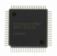
DF2134AFA20V Renesas Electronics America, DF2134AFA20V Datasheet - Page 291

DF2134AFA20V
Manufacturer Part Number
DF2134AFA20V
Description
IC H8S/2100 MCU FLASH 80QFP
Manufacturer
Renesas Electronics America
Series
H8® H8S/2100r
Datasheets
1.HEWH8E10A.pdf
(19 pages)
2.D12312SVTE25V.pdf
(341 pages)
3.DF2134AFA20V.pdf
(1063 pages)
Specifications of DF2134AFA20V
Core Processor
H8S/2000
Core Size
16-Bit
Speed
20MHz
Connectivity
IrDA, SCI
Peripherals
POR, PWM, WDT
Number Of I /o
58
Program Memory Size
128KB (128K x 8)
Program Memory Type
FLASH
Ram Size
4K x 8
Voltage - Supply (vcc/vdd)
4 V ~ 5.5 V
Data Converters
A/D 8x10b; D/A 2x8b
Oscillator Type
Internal
Operating Temperature
-20°C ~ 75°C
Package / Case
80-QFP
For Use With
3DK2166 - DEV EVAL KIT H8S/2166
Lead Free Status / RoHS Status
Lead free / RoHS Compliant
Eeprom Size
-
Available stocks
Company
Part Number
Manufacturer
Quantity
Price
Company:
Part Number:
DF2134AFA20V
Manufacturer:
Renesas Electronics America
Quantity:
10 000
- Current page: 291 of 1063
- Download datasheet (6Mb)
8.10.2
Table 8.19 summarizes the port 9 registers.
Table 8.19 Port 9 Registers
Notes: 1. Lower 16 bits of the address.
Port 9 Data Direction Register (P9DDR)
P9DDR is an 8-bit write-only register, the individual bits of which specify input or output for the
pins of port 9. P9DDR cannot be read; if it is, an undefined value will be returned.
P9DDR is initialized to H'40 (mode 1) or H'00 (modes 2 and 3) by a reset and in hardware standby
mode. It retains its prior state in software standby mode.
Name
Port 9 data direction register
Port 9 data register
Mode 1
Modes 2 and 3
Bit
Initial value
Read/Write
Initial value
Read/Write
Modes 1, 2, and 3 (EXPE = 1)
Pin P97 functions as a bus control input (WAIT), the IIC0 I/O pin (SDA0), or an I/O port,
according to the wait mode setting. When P97 functions as an I/O port, it becomes an output
port when P97DDR is set to 1, and an input port when P97DDR is cleared to 0.
Pin P96 functions as the output pin when P96DDR is set to 1, and as the subclock input
(EXCL) or an input port when P96DDR is cleared to 0.
Pins P95 to P93 automatically become bus control outputs (AS/IOS, WR, RD), regardless of
the input/output direction indicated by P95DDR to P93DDR.
Pins P92 and P90 become output ports when P92DDR and P90DDR are set to 1, and input
ports when P92DDR and P91DDR are cleared to 0.
2. Initial value depends on the mode.
Register Configuration
P97DDR P96DDR P95DDR P94DDR P93DDR P92DDR P91DDR P90DDR
W
W
7
0
0
W
W
6
1
0
Abbreviation
P9DDR
P9DR
W
W
5
0
0
W
W
4
0
0
R/W
W
R/W
Rev. 4.00 Jun 06, 2006 page 235 of 1004
W
W
3
0
0
Initial Value
H'40/H'00 *
H'00
W
W
2
0
0
2
Section 8 I/O Ports
REJ09B0301-0400
Address *
H'FFC0
H'FFC1
W
W
1
0
0
1
W
W
0
0
0
Related parts for DF2134AFA20V
Image
Part Number
Description
Manufacturer
Datasheet
Request
R

Part Number:
Description:
KIT STARTER FOR M16C/29
Manufacturer:
Renesas Electronics America
Datasheet:

Part Number:
Description:
KIT STARTER FOR R8C/2D
Manufacturer:
Renesas Electronics America
Datasheet:

Part Number:
Description:
R0K33062P STARTER KIT
Manufacturer:
Renesas Electronics America
Datasheet:

Part Number:
Description:
KIT STARTER FOR R8C/23 E8A
Manufacturer:
Renesas Electronics America
Datasheet:

Part Number:
Description:
KIT STARTER FOR R8C/25
Manufacturer:
Renesas Electronics America
Datasheet:

Part Number:
Description:
KIT STARTER H8S2456 SHARPE DSPLY
Manufacturer:
Renesas Electronics America
Datasheet:

Part Number:
Description:
KIT STARTER FOR R8C38C
Manufacturer:
Renesas Electronics America
Datasheet:

Part Number:
Description:
KIT STARTER FOR R8C35C
Manufacturer:
Renesas Electronics America
Datasheet:

Part Number:
Description:
KIT STARTER FOR R8CL3AC+LCD APPS
Manufacturer:
Renesas Electronics America
Datasheet:

Part Number:
Description:
KIT STARTER FOR RX610
Manufacturer:
Renesas Electronics America
Datasheet:

Part Number:
Description:
KIT STARTER FOR R32C/118
Manufacturer:
Renesas Electronics America
Datasheet:

Part Number:
Description:
KIT DEV RSK-R8C/26-29
Manufacturer:
Renesas Electronics America
Datasheet:

Part Number:
Description:
KIT STARTER FOR SH7124
Manufacturer:
Renesas Electronics America
Datasheet:

Part Number:
Description:
KIT STARTER FOR H8SX/1622
Manufacturer:
Renesas Electronics America
Datasheet:

Part Number:
Description:
KIT DEV FOR SH7203
Manufacturer:
Renesas Electronics America
Datasheet:


