DF2134AFA20V Renesas Electronics America, DF2134AFA20V Datasheet - Page 631
DF2134AFA20V
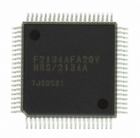
Manufacturer Part Number
DF2134AFA20V
Description
IC H8S/2100 MCU FLASH 80QFP
Manufacturer
Renesas Electronics America
Series
H8® H8S/2100r
Datasheets
1.HEWH8E10A.pdf
(19 pages)
2.D12312SVTE25V.pdf
(341 pages)
3.DF2134AFA20V.pdf
(1063 pages)
Specifications of DF2134AFA20V
Core Processor
H8S/2000
Core Size
16-Bit
Speed
20MHz
Connectivity
IrDA, SCI
Peripherals
POR, PWM, WDT
Number Of I /o
58
Program Memory Size
128KB (128K x 8)
Program Memory Type
FLASH
Ram Size
4K x 8
Voltage - Supply (vcc/vdd)
4 V ~ 5.5 V
Data Converters
A/D 8x10b; D/A 2x8b
Oscillator Type
Internal
Operating Temperature
-20°C ~ 75°C
Package / Case
80-QFP
For Use With
3DK2166 - DEV EVAL KIT H8S/2166
Lead Free Status / RoHS Status
Lead free / RoHS Compliant
Eeprom Size
-
Available stocks
Company
Part Number
Manufacturer
Quantity
Price
Company:

Part Number:
DF2134AFA20V
Manufacturer:
Renesas Electronics America
Quantity:
10 000


20.3
20.3.1
When the RAME bit is set to 1, accesses to H8S/2138, H8S/2134, and H8S/2133 addresses
H'(FF)E080 to H'(FF)EFFF and H'(FF)FF00 to H'(FF)FF7F, and H8S/2137, H8S/2132, and
H8S/2130 addresses H'(FF)E880 to H'(FF)EFFF and H'(FF)FF00 to H'(FF)FF7F, are directed to
the on-chip RAM. When the RAME bit is cleared to 0, accesses to addresses H'(FF)E080 to
H'(FF)EFFF and H'(FF)FF00 to H'(FF)FF7F, are directed to the off-chip address space.
Since the on-chip RAM is connected to the bus master by a 16-bit data bus, it can be written to
and read in byte or word units. Each type of access is performed in one state.
Even addresses use the upper 8 bits, and odd addresses use the lower 8 bits. Word data must start
at an even address.
20.3.2
When the RAME bit is set to 1, accesses to H8S/2138, H8S/2134, and H8S/2133 addresses
H'(FF)E080 to H'(FF)EFFF and H'(FF)FF00 to H'(FF)FF7F, and H8S/2137, H8S/2132, and
H8S/2130 addresses H'(FF)E880 to H'(FF)EFFF and H'(FF)FF00 to H'(FF)FF7F, are directed to
the on-chip RAM. When the RAME bit is cleared to 0, the on-chip RAM is not accessed.
Undefined values are read from these bits, and writing is invalid.
Since the on-chip RAM is connected to the bus master by a 16-bit data bus, it can be written to
and read in byte or word units. Each type of access is performed in one state.
Even addresses use the upper 8 bits, and odd addresses use the lower 8 bits. Word data must start
at an even address.
Operation
Expanded Mode (Modes 1, 2, and 3 (EXPE = 1))
Single-Chip Mode (Modes 2 and 3 (EXPE = 0))
Rev. 4.00 Jun 06, 2006 page 575 of 1004
REJ09B0301-0400
Section 20 RAM
Related parts for DF2134AFA20V
Image
Part Number
Description
Manufacturer
Datasheet
Request
R

Part Number:
Description:
KIT STARTER FOR M16C/29
Manufacturer:
Renesas Electronics America
Datasheet:

Part Number:
Description:
KIT STARTER FOR R8C/2D
Manufacturer:
Renesas Electronics America
Datasheet:

Part Number:
Description:
R0K33062P STARTER KIT
Manufacturer:
Renesas Electronics America
Datasheet:

Part Number:
Description:
KIT STARTER FOR R8C/23 E8A
Manufacturer:
Renesas Electronics America
Datasheet:

Part Number:
Description:
KIT STARTER FOR R8C/25
Manufacturer:
Renesas Electronics America
Datasheet:

Part Number:
Description:
KIT STARTER H8S2456 SHARPE DSPLY
Manufacturer:
Renesas Electronics America
Datasheet:

Part Number:
Description:
KIT STARTER FOR R8C38C
Manufacturer:
Renesas Electronics America
Datasheet:

Part Number:
Description:
KIT STARTER FOR R8C35C
Manufacturer:
Renesas Electronics America
Datasheet:

Part Number:
Description:
KIT STARTER FOR R8CL3AC+LCD APPS
Manufacturer:
Renesas Electronics America
Datasheet:
Part Number:
Description:
KIT STARTER FOR RX610
Manufacturer:
Renesas Electronics America
Datasheet:

Part Number:
Description:
KIT STARTER FOR R32C/118
Manufacturer:
Renesas Electronics America
Datasheet:

Part Number:
Description:
KIT DEV RSK-R8C/26-29
Manufacturer:
Renesas Electronics America
Datasheet:

Part Number:
Description:
KIT STARTER FOR SH7124
Manufacturer:
Renesas Electronics America
Datasheet:

Part Number:
Description:
KIT STARTER FOR H8SX/1622
Manufacturer:
Renesas Electronics America
Datasheet:

Part Number:
Description:
KIT DEV FOR SH7203
Manufacturer:
Renesas Electronics America
Datasheet: