DF2134AFA20V Renesas Electronics America, DF2134AFA20V Datasheet - Page 537
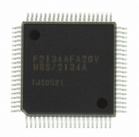
DF2134AFA20V
Manufacturer Part Number
DF2134AFA20V
Description
IC H8S/2100 MCU FLASH 80QFP
Manufacturer
Renesas Electronics America
Series
H8® H8S/2100r
Datasheets
1.HEWH8E10A.pdf
(19 pages)
2.D12312SVTE25V.pdf
(341 pages)
3.DF2134AFA20V.pdf
(1063 pages)
Specifications of DF2134AFA20V
Core Processor
H8S/2000
Core Size
16-Bit
Speed
20MHz
Connectivity
IrDA, SCI
Peripherals
POR, PWM, WDT
Number Of I /o
58
Program Memory Size
128KB (128K x 8)
Program Memory Type
FLASH
Ram Size
4K x 8
Voltage - Supply (vcc/vdd)
4 V ~ 5.5 V
Data Converters
A/D 8x10b; D/A 2x8b
Oscillator Type
Internal
Operating Temperature
-20°C ~ 75°C
Package / Case
80-QFP
For Use With
3DK2166 - DEV EVAL KIT H8S/2166
Lead Free Status / RoHS Status
Lead free / RoHS Compliant
Eeprom Size
-
Available stocks
Company
Part Number
Manufacturer
Quantity
Price
Company:

Part Number:
DF2134AFA20V
Manufacturer:
Renesas Electronics America
Quantity:
10 000


Bits 6 and 5—I
to CKS0 in ICMR of IIC1, select the transfer rate in master mode. For details, see section 16.2.4,
I
Bit 4—I
registers (ICCR, ICSR, ICDR/SARX, ICMR/SAR).
Bit 3—Flash Memory Control Register Enable (FLSHE): Controls the operation of the flash
memory in F-ZTAT versions. For details, see section 21, ROM (Mask ROM Version, H8S/2138
F-ZTAT, H8S/2134 F-ZTAT, and H8S/2132 F-ZTAT), and section 22, ROM (H8S/2138 F-ZTAT
A-Mask Version, H8S/2134 F-ZTAT A-Mask Version).
Bit 2—Reserved: Do not write 1 to this bit.
Bits 1 and 0—Internal Clock Source Select 1 and 0 (ICKS1, ICSK0): These bits, together with
bits CKS2 to CKS0 in TCR, select the clock input to the timer counters (TCNT). For details, see
section 12.2.4, Timer Control Register (TCR).
16.2.8
DDCSWR is an 8-bit readable/writable register that controls the IIC channel 0 automatic format
switching function.
DDCSWR is initialized to H'0F by a reset and in hardware standby mode.
Bit 4
IICE
0
1
2
C Bus Mode Register (ICMR).
Bit
Initial value
Read/Write
Notes: 1. Only 0 can be written, to clear the flag.
2
C Master Enable (IICE): Controls CPU access to the I
DDC Switch Register (DDCSWR)
2. Always read as 1.
Description
CPU access to I
CPU access to I
2
C Transfer Select 1 and 0 (IICX1, IICX0): These bits, together with bits CKS2
SWE
R/W
7
0
2
2
C bus interface data and control registers is disabled
C bus interface data and control registers is enabled
R/W
SW
6
0
R/W
IE
5
0
Section 16 I
R/(W) *
IF
4
0
1
Rev. 4.00 Jun 06, 2006 page 481 of 1004
2
C Bus Interface [H8S/2138 Group Option]
CLR3
W *
3
1
2
2
C bus interface data and control
CLR2
W *
2
1
2
CLR1
W *
REJ09B0301-0400
1
1
2
(Initial value)
CLR0
W *
0
1
2
Related parts for DF2134AFA20V
Image
Part Number
Description
Manufacturer
Datasheet
Request
R

Part Number:
Description:
KIT STARTER FOR M16C/29
Manufacturer:
Renesas Electronics America
Datasheet:

Part Number:
Description:
KIT STARTER FOR R8C/2D
Manufacturer:
Renesas Electronics America
Datasheet:

Part Number:
Description:
R0K33062P STARTER KIT
Manufacturer:
Renesas Electronics America
Datasheet:

Part Number:
Description:
KIT STARTER FOR R8C/23 E8A
Manufacturer:
Renesas Electronics America
Datasheet:

Part Number:
Description:
KIT STARTER FOR R8C/25
Manufacturer:
Renesas Electronics America
Datasheet:

Part Number:
Description:
KIT STARTER H8S2456 SHARPE DSPLY
Manufacturer:
Renesas Electronics America
Datasheet:

Part Number:
Description:
KIT STARTER FOR R8C38C
Manufacturer:
Renesas Electronics America
Datasheet:

Part Number:
Description:
KIT STARTER FOR R8C35C
Manufacturer:
Renesas Electronics America
Datasheet:

Part Number:
Description:
KIT STARTER FOR R8CL3AC+LCD APPS
Manufacturer:
Renesas Electronics America
Datasheet:
Part Number:
Description:
KIT STARTER FOR RX610
Manufacturer:
Renesas Electronics America
Datasheet:

Part Number:
Description:
KIT STARTER FOR R32C/118
Manufacturer:
Renesas Electronics America
Datasheet:

Part Number:
Description:
KIT DEV RSK-R8C/26-29
Manufacturer:
Renesas Electronics America
Datasheet:

Part Number:
Description:
KIT STARTER FOR SH7124
Manufacturer:
Renesas Electronics America
Datasheet:

Part Number:
Description:
KIT STARTER FOR H8SX/1622
Manufacturer:
Renesas Electronics America
Datasheet:

Part Number:
Description:
KIT DEV FOR SH7203
Manufacturer:
Renesas Electronics America
Datasheet: