DF2134AFA20V Renesas Electronics America, DF2134AFA20V Datasheet - Page 54
DF2134AFA20V
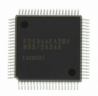
Manufacturer Part Number
DF2134AFA20V
Description
IC H8S/2100 MCU FLASH 80QFP
Manufacturer
Renesas Electronics America
Series
H8® H8S/2100r
Datasheets
1.HEWH8E10A.pdf
(19 pages)
2.D12312SVTE25V.pdf
(341 pages)
3.DF2134AFA20V.pdf
(1063 pages)
Specifications of DF2134AFA20V
Core Processor
H8S/2000
Core Size
16-Bit
Speed
20MHz
Connectivity
IrDA, SCI
Peripherals
POR, PWM, WDT
Number Of I /o
58
Program Memory Size
128KB (128K x 8)
Program Memory Type
FLASH
Ram Size
4K x 8
Voltage - Supply (vcc/vdd)
4 V ~ 5.5 V
Data Converters
A/D 8x10b; D/A 2x8b
Oscillator Type
Internal
Operating Temperature
-20°C ~ 75°C
Package / Case
80-QFP
For Use With
3DK2166 - DEV EVAL KIT H8S/2166
Lead Free Status / RoHS Status
Lead free / RoHS Compliant
Eeprom Size
-
Available stocks
Company
Part Number
Manufacturer
Quantity
Price
Company:

Part Number:
DF2134AFA20V
Manufacturer:
Renesas Electronics America
Quantity:
10 000


Table 24.3
Table 24.4
Table 24.5
Section 25 Electrical Characteristics
Table 25.1
Table 25.1
Table 25.1
Table 25.1
Table 25.2
Table 25.3
Table 25.3
Table 25.3
Table 25.4
Table 25.5
Table 25.6
Table 25.7
Table 25.8
Table 25.9
Table 25.9
Table 25.10 I
Table 25.11 A/D Conversion Characteristics
Table 25.12 A/D Conversion Characteristics
Table 25.13 D/A Conversion Characteristics ............................................................................. 729
Table 25.14 Flash Memory Characteristics (Programming/Erasing Operating Range) ............. 730
Table 25.15 Absolute Maximum Ratings................................................................................... 733
Table 25.16 DC Characteristics (1) ............................................................................................ 734
Table 25.16 DC Characteristics (2) ............................................................................................ 737
Table 25.16 DC Characteristics (3) ............................................................................................ 740
Table 25.17 Permissible Output Currents .................................................................................. 743
Table 25.18 Bus Drive Characteristics ....................................................................................... 744
Table 25.19 Clock Timing ......................................................................................................... 745
Table 25.20 Control Signal Timing............................................................................................ 746
Table 25.21 Bus Timing............................................................................................................. 747
Table 25.22 Timing of On-Chip Supporting Modules (1).......................................................... 749
Table 25.22 Timing of On-Chip Supporting Modules (2).......................................................... 751
Table 25.23 I
Table 25.24 A/D Conversion Characteristics
Rev. 4.00 Jun 06, 2006 page lii of liv
Power-Down State Registers.................................................................................. 685
MSTP Bits and Corresponding On-Chip Supporting Modules .............................. 694
Oscillation Settling Time Settings.......................................................................... 696
Power Supply Voltage and Operating Range (1) (F-ZTAT Products) ................... 703
Power Supply Voltage and Operating Range (2) (F-ZTAT A-Mask Products) ..... 704
Power Supply Voltage and Operating Range (3) (Mask-ROM Products).............. 704
Power Supply Voltage and Operating Range (4) (Mask-ROM Products).............. 705
Absolute Maximum Ratings................................................................................... 706
DC Characteristics (1) ............................................................................................ 707
DC Characteristics (2) ............................................................................................ 710
DC Characteristics (3) ............................................................................................ 713
Permissible Output Currents .................................................................................. 716
Bus Drive Characteristics ....................................................................................... 718
Clock Timing ......................................................................................................... 719
Control Signal Timing............................................................................................ 720
Bus Timing............................................................................................................. 721
Timing of On-Chip Supporting Modules (1).......................................................... 723
Timing of On-Chip Supporting Modules (2).......................................................... 725
(AN7 to AN0 Input: 134/266-State Conversion) ................................................... 727
(CIN7 to CIN0 Input: 134/266-State Conversion) ................................................. 728
(AN7 to AN0 Input: 134/266-State Conversion) ................................................... 753
2
2
C Bus Timing....................................................................................................... 726
C Bus Timing....................................................................................................... 752
Related parts for DF2134AFA20V
Image
Part Number
Description
Manufacturer
Datasheet
Request
R

Part Number:
Description:
KIT STARTER FOR M16C/29
Manufacturer:
Renesas Electronics America
Datasheet:

Part Number:
Description:
KIT STARTER FOR R8C/2D
Manufacturer:
Renesas Electronics America
Datasheet:

Part Number:
Description:
R0K33062P STARTER KIT
Manufacturer:
Renesas Electronics America
Datasheet:

Part Number:
Description:
KIT STARTER FOR R8C/23 E8A
Manufacturer:
Renesas Electronics America
Datasheet:

Part Number:
Description:
KIT STARTER FOR R8C/25
Manufacturer:
Renesas Electronics America
Datasheet:

Part Number:
Description:
KIT STARTER H8S2456 SHARPE DSPLY
Manufacturer:
Renesas Electronics America
Datasheet:

Part Number:
Description:
KIT STARTER FOR R8C38C
Manufacturer:
Renesas Electronics America
Datasheet:

Part Number:
Description:
KIT STARTER FOR R8C35C
Manufacturer:
Renesas Electronics America
Datasheet:

Part Number:
Description:
KIT STARTER FOR R8CL3AC+LCD APPS
Manufacturer:
Renesas Electronics America
Datasheet:
Part Number:
Description:
KIT STARTER FOR RX610
Manufacturer:
Renesas Electronics America
Datasheet:

Part Number:
Description:
KIT STARTER FOR R32C/118
Manufacturer:
Renesas Electronics America
Datasheet:

Part Number:
Description:
KIT DEV RSK-R8C/26-29
Manufacturer:
Renesas Electronics America
Datasheet:

Part Number:
Description:
KIT STARTER FOR SH7124
Manufacturer:
Renesas Electronics America
Datasheet:

Part Number:
Description:
KIT STARTER FOR H8SX/1622
Manufacturer:
Renesas Electronics America
Datasheet:

Part Number:
Description:
KIT DEV FOR SH7203
Manufacturer:
Renesas Electronics America
Datasheet: