DF2134AFA20V Renesas Electronics America, DF2134AFA20V Datasheet - Page 718
DF2134AFA20V
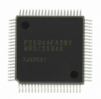
Manufacturer Part Number
DF2134AFA20V
Description
IC H8S/2100 MCU FLASH 80QFP
Manufacturer
Renesas Electronics America
Series
H8® H8S/2100r
Datasheets
1.HEWH8E10A.pdf
(19 pages)
2.D12312SVTE25V.pdf
(341 pages)
3.DF2134AFA20V.pdf
(1063 pages)
Specifications of DF2134AFA20V
Core Processor
H8S/2000
Core Size
16-Bit
Speed
20MHz
Connectivity
IrDA, SCI
Peripherals
POR, PWM, WDT
Number Of I /o
58
Program Memory Size
128KB (128K x 8)
Program Memory Type
FLASH
Ram Size
4K x 8
Voltage - Supply (vcc/vdd)
4 V ~ 5.5 V
Data Converters
A/D 8x10b; D/A 2x8b
Oscillator Type
Internal
Operating Temperature
-20°C ~ 75°C
Package / Case
80-QFP
For Use With
3DK2166 - DEV EVAL KIT H8S/2166
Lead Free Status / RoHS Status
Lead free / RoHS Compliant
Eeprom Size
-
Available stocks
Company
Part Number
Manufacturer
Quantity
Price
Company:

Part Number:
DF2134AFA20V
Manufacturer:
Renesas Electronics America
Quantity:
10 000


Section 22 ROM
Notes on Use of Auto-Program Mode
Rev. 4.00 Jun 06, 2006 page 662 of 1004
REJ09B0301-0400
FA17 to FA0
FO7 to FO0
In auto-program mode, 128 bytes are programmed simultaneously. This should be carried out
by executing 128 consecutive byte transfers.
A 128-byte data transfer is necessary even when programming fewer than 128 bytes. In this
case, H'FF data must be written to the extra addresses.
The lower 8 bits of the transfer address must be H'00 or H'80. If a value other than an effective
address is input, processing will switch to a memory write operation but a write error will be
flagged.
Memory address transfer is performed in the second cycle (figure 22.20). Do not perform
transfer after the second cycle.
Do not perform a command write during a programming operation.
Perform one auto-programming operation for a 128-byte block for each address.
Characteristics are not guaranteed for two or more programming operations.
Confirm normal end of auto-programming by checking FO6. Alternatively, status read mode
can also be used for this purpose (FO7 status polling uses the auto-program operation end
identification pin).
The status polling FO6 and FO7 pin information is retained until the next command write.
Until the next command write is performed, reading is possible by enabling CE and OE.
FO7
FO6
WE
OE
CE
t
ces
t
f
(H8S/2138 F-ZTAT A-Mask Version, H8S/2134 F-ZTAT A-Mask Version)
Figure 22.20 Auto-Program Mode Timing Waveforms
t
wep
t
H'40
ds
t
t
ceh
dh
t
r
t
nxtc
t
as
Address
stable
Data
t
ah
1 byte to 128 bytes
Data transfer
Data
t
write
Programming wait
Programming operation
end identification signal
Programming normal
end identification signal
t
wsts
(1 to 3000 ms)
t
spa
FO5 to FO0 = 0
t
nxtc
Related parts for DF2134AFA20V
Image
Part Number
Description
Manufacturer
Datasheet
Request
R

Part Number:
Description:
KIT STARTER FOR M16C/29
Manufacturer:
Renesas Electronics America
Datasheet:

Part Number:
Description:
KIT STARTER FOR R8C/2D
Manufacturer:
Renesas Electronics America
Datasheet:

Part Number:
Description:
R0K33062P STARTER KIT
Manufacturer:
Renesas Electronics America
Datasheet:

Part Number:
Description:
KIT STARTER FOR R8C/23 E8A
Manufacturer:
Renesas Electronics America
Datasheet:

Part Number:
Description:
KIT STARTER FOR R8C/25
Manufacturer:
Renesas Electronics America
Datasheet:

Part Number:
Description:
KIT STARTER H8S2456 SHARPE DSPLY
Manufacturer:
Renesas Electronics America
Datasheet:

Part Number:
Description:
KIT STARTER FOR R8C38C
Manufacturer:
Renesas Electronics America
Datasheet:

Part Number:
Description:
KIT STARTER FOR R8C35C
Manufacturer:
Renesas Electronics America
Datasheet:

Part Number:
Description:
KIT STARTER FOR R8CL3AC+LCD APPS
Manufacturer:
Renesas Electronics America
Datasheet:
Part Number:
Description:
KIT STARTER FOR RX610
Manufacturer:
Renesas Electronics America
Datasheet:

Part Number:
Description:
KIT STARTER FOR R32C/118
Manufacturer:
Renesas Electronics America
Datasheet:

Part Number:
Description:
KIT DEV RSK-R8C/26-29
Manufacturer:
Renesas Electronics America
Datasheet:

Part Number:
Description:
KIT STARTER FOR SH7124
Manufacturer:
Renesas Electronics America
Datasheet:

Part Number:
Description:
KIT STARTER FOR H8SX/1622
Manufacturer:
Renesas Electronics America
Datasheet:

Part Number:
Description:
KIT DEV FOR SH7203
Manufacturer:
Renesas Electronics America
Datasheet: