DF2134AFA20V Renesas Electronics America, DF2134AFA20V Datasheet - Page 43
DF2134AFA20V
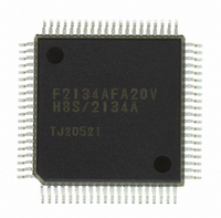
Manufacturer Part Number
DF2134AFA20V
Description
IC H8S/2100 MCU FLASH 80QFP
Manufacturer
Renesas Electronics America
Series
H8® H8S/2100r
Datasheets
1.HEWH8E10A.pdf
(19 pages)
2.D12312SVTE25V.pdf
(341 pages)
3.DF2134AFA20V.pdf
(1063 pages)
Specifications of DF2134AFA20V
Core Processor
H8S/2000
Core Size
16-Bit
Speed
20MHz
Connectivity
IrDA, SCI
Peripherals
POR, PWM, WDT
Number Of I /o
58
Program Memory Size
128KB (128K x 8)
Program Memory Type
FLASH
Ram Size
4K x 8
Voltage - Supply (vcc/vdd)
4 V ~ 5.5 V
Data Converters
A/D 8x10b; D/A 2x8b
Oscillator Type
Internal
Operating Temperature
-20°C ~ 75°C
Package / Case
80-QFP
For Use With
3DK2166 - DEV EVAL KIT H8S/2166
Lead Free Status / RoHS Status
Lead free / RoHS Compliant
Eeprom Size
-
Available stocks
Company
Part Number
Manufacturer
Quantity
Price
Company:

Part Number:
DF2134AFA20V
Manufacturer:
Renesas Electronics America
Quantity:
10 000


Figure 16.16
Figure 16.17
Figure 16.18
Figure 16.19
Figure 16.20
Figure 16.21
Figure 16.22
Figure 16.23
Figure 16.24
Figure 16.25
Figure 16.26
Figure 16.27
Section 17 Host Interface [H8S/2138 Group]
Figure 17.1
Figure 17.2
Figure 17.3
Section 18 D/A Converter
Figure 18.1
Figure 18.2
Section 19 A/D Converter
Figure 19.1
Figure 19.2
Figure 19.3
Figure 19.4
Figure 19.5
Figure 19.6
Figure 19.7
Figure 19.8
Figure 19.9
Figure 19.10
Figure 19.11
Section 20 RAM
Figure 20.1
Flowchart for Slave Receive Mode (Example).................................................. 503
Flowchart for Slave Transmit Mode (Example) ................................................ 504
Points for Attention Concerning Reading of Master Receive Data ................... 511
Flowchart and Timing of Start Condition Instruction Issuance
for Retransmission............................................................................................. 512
Timing of Stop Condition Issuance ................................................................... 513
IRIC Flag Clear Timing on WAIT Operation ................................................... 514
ICDR Read and ICCR Access Timing in Slave Transmit Mode....................... 515
TRS Bit Setting Timing in Slave Mode............................................................. 516
Diagram of Erroneous Operation when Arbitration is Lost............................... 517
Note on Interrupt Occurrence in Slave Mode after ACKB = 1 Reception ........ 519
Notes on ICDR Reading with TRS = 1 Setting in Master Mode....................... 521
Notes on ICDR Writing with TRS = 0 Setting in Slave Mode .......................... 521
Block Diagram of Host Interface....................................................................... 524
GA20 Output ..................................................................................................... 538
HIRQ Output Flowchart .................................................................................... 542
Block Diagram of D/A Converter...................................................................... 544
D/A Conversion (Example) ............................................................................... 549
Block Diagram of A/D Converter...................................................................... 552
ADDR Access Operation (Reading H'AA40) ................................................... 561
Example of A/D Converter Operation (Single Mode, Channel 1 Selected) ...... 563
Example of A/D Converter Operation (Scan Mode, Channels AN0 to AN2
Selected) ............................................................................................................ 565
A/D Conversion Timing .................................................................................... 566
External Trigger Input Timing .......................................................................... 567
Example of Analog Input Protection Circuit ..................................................... 569
Analog Input Pin Equivalent Circuit ................................................................. 569
A/D Conversion Precision Definitions (1)......................................................... 571
A/D Conversion Precision Definitions (2)......................................................... 571
Example of Analog Input Circuit ...................................................................... 572
Block Diagram of RAM (H8S/2138, H8S/2134, H8S/2133) ............................ 573
Rev. 4.00 Jun 06, 2006 page xli of liv
Related parts for DF2134AFA20V
Image
Part Number
Description
Manufacturer
Datasheet
Request
R

Part Number:
Description:
KIT STARTER FOR M16C/29
Manufacturer:
Renesas Electronics America
Datasheet:

Part Number:
Description:
KIT STARTER FOR R8C/2D
Manufacturer:
Renesas Electronics America
Datasheet:

Part Number:
Description:
R0K33062P STARTER KIT
Manufacturer:
Renesas Electronics America
Datasheet:

Part Number:
Description:
KIT STARTER FOR R8C/23 E8A
Manufacturer:
Renesas Electronics America
Datasheet:

Part Number:
Description:
KIT STARTER FOR R8C/25
Manufacturer:
Renesas Electronics America
Datasheet:

Part Number:
Description:
KIT STARTER H8S2456 SHARPE DSPLY
Manufacturer:
Renesas Electronics America
Datasheet:

Part Number:
Description:
KIT STARTER FOR R8C38C
Manufacturer:
Renesas Electronics America
Datasheet:

Part Number:
Description:
KIT STARTER FOR R8C35C
Manufacturer:
Renesas Electronics America
Datasheet:

Part Number:
Description:
KIT STARTER FOR R8CL3AC+LCD APPS
Manufacturer:
Renesas Electronics America
Datasheet:
Part Number:
Description:
KIT STARTER FOR RX610
Manufacturer:
Renesas Electronics America
Datasheet:

Part Number:
Description:
KIT STARTER FOR R32C/118
Manufacturer:
Renesas Electronics America
Datasheet:

Part Number:
Description:
KIT DEV RSK-R8C/26-29
Manufacturer:
Renesas Electronics America
Datasheet:

Part Number:
Description:
KIT STARTER FOR SH7124
Manufacturer:
Renesas Electronics America
Datasheet:

Part Number:
Description:
KIT STARTER FOR H8SX/1622
Manufacturer:
Renesas Electronics America
Datasheet:

Part Number:
Description:
KIT DEV FOR SH7203
Manufacturer:
Renesas Electronics America
Datasheet: