DF2134AFA20V Renesas Electronics America, DF2134AFA20V Datasheet - Page 566
DF2134AFA20V
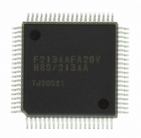
Manufacturer Part Number
DF2134AFA20V
Description
IC H8S/2100 MCU FLASH 80QFP
Manufacturer
Renesas Electronics America
Series
H8® H8S/2100r
Datasheets
1.HEWH8E10A.pdf
(19 pages)
2.D12312SVTE25V.pdf
(341 pages)
3.DF2134AFA20V.pdf
(1063 pages)
Specifications of DF2134AFA20V
Core Processor
H8S/2000
Core Size
16-Bit
Speed
20MHz
Connectivity
IrDA, SCI
Peripherals
POR, PWM, WDT
Number Of I /o
58
Program Memory Size
128KB (128K x 8)
Program Memory Type
FLASH
Ram Size
4K x 8
Voltage - Supply (vcc/vdd)
4 V ~ 5.5 V
Data Converters
A/D 8x10b; D/A 2x8b
Oscillator Type
Internal
Operating Temperature
-20°C ~ 75°C
Package / Case
80-QFP
For Use With
3DK2166 - DEV EVAL KIT H8S/2166
Lead Free Status / RoHS Status
Lead free / RoHS Compliant
Eeprom Size
-
Available stocks
Company
Part Number
Manufacturer
Quantity
Price
Company:

Part Number:
DF2134AFA20V
Manufacturer:
Renesas Electronics America
Quantity:
10 000


Section 16 I
Item
t
Notes: 1. Does not meet the I
Rev. 4.00 Jun 06, 2006 page 510 of 1004
REJ09B0301-0400
SDAHO
Note on ICDR Read at End of Master Reception
To halt reception at the end of a receive operation in master receive mode, set the TRS bit to 1
and write 0 to BBSY and SCP in ICCR. This changes SDA from low to high when SCL is
high, and generates the stop condition. After this, receive data can be read by means of an
ICDR read, but if data remains in the buffer the ICDRS receive data will not be transferred to
ICDR, and so it will not be possible to read the second byte of data.
If it is necessary to read the second byte of data, issue the stop condition in master receive
mode (i.e. with the TRS bit cleared to 0). When reading the receive data, first confirm that the
BBSY bit in the ICCR register is cleared to 0, the stop condition has been generated, and the
bus has been released, then read the ICDR register with TRS cleared to 0.
Note that if the receive data (ICDR data) is read in the interval between execution of the
instruction for issuance of the stop condition (writing of 0 to BBSY and SCP in ICCR) and the
actual generation of the stop condition, the clock may not be output correctly in subsequent
master transmission.
2. Value when the IICX bit is set to 1. When the IICX bit is cleared to 0, the value is (t
3. Calculated using the I
t
Indication
3t
cyc
cyc
is necessary: (a) secure a start/stop condition issuance interval; (b) adjust the rise and
fall times by means of a pull-up resistor and capacitive load; (c) reduce the transfer rate;
(d) select slave devices whose input timing permits this output timing.
The values in the above table will vary depending on the settings of the IICX bit and bits
CKS0 to CKS2. Depending on the frequency it may not be possible to achieve the
maximum transfer rate; therefore, whether or not the I
met must be determined in accordance with the actual setting conditions.
6t
speed mode: 1300 ns min.).
2
cyc
C Bus Interface [H8S/2138 Group Option]
).
Standard
mode
High-speed
mode
2
C bus interface specification. Remedial action such as the following
2
t
Influence
(Max.)
0
0
C bus specification values (standard mode: 4700 ns min.; high-
Time Indication (at Maximum Transfer Rate) [ns]
Sr
/t
Sf
I
Specifi-
cation
(Min.)
0
0
2
C Bus
5 MHz
600
600
=
8 MHz
375
375
2
=
C bus interface specifications are
300
300
10 MHz
=
16 MHz
188
188
=
20 MHz
150
150
=
SCLL
–
Related parts for DF2134AFA20V
Image
Part Number
Description
Manufacturer
Datasheet
Request
R

Part Number:
Description:
KIT STARTER FOR M16C/29
Manufacturer:
Renesas Electronics America
Datasheet:

Part Number:
Description:
KIT STARTER FOR R8C/2D
Manufacturer:
Renesas Electronics America
Datasheet:

Part Number:
Description:
R0K33062P STARTER KIT
Manufacturer:
Renesas Electronics America
Datasheet:

Part Number:
Description:
KIT STARTER FOR R8C/23 E8A
Manufacturer:
Renesas Electronics America
Datasheet:

Part Number:
Description:
KIT STARTER FOR R8C/25
Manufacturer:
Renesas Electronics America
Datasheet:

Part Number:
Description:
KIT STARTER H8S2456 SHARPE DSPLY
Manufacturer:
Renesas Electronics America
Datasheet:

Part Number:
Description:
KIT STARTER FOR R8C38C
Manufacturer:
Renesas Electronics America
Datasheet:

Part Number:
Description:
KIT STARTER FOR R8C35C
Manufacturer:
Renesas Electronics America
Datasheet:

Part Number:
Description:
KIT STARTER FOR R8CL3AC+LCD APPS
Manufacturer:
Renesas Electronics America
Datasheet:
Part Number:
Description:
KIT STARTER FOR RX610
Manufacturer:
Renesas Electronics America
Datasheet:

Part Number:
Description:
KIT STARTER FOR R32C/118
Manufacturer:
Renesas Electronics America
Datasheet:

Part Number:
Description:
KIT DEV RSK-R8C/26-29
Manufacturer:
Renesas Electronics America
Datasheet:

Part Number:
Description:
KIT STARTER FOR SH7124
Manufacturer:
Renesas Electronics America
Datasheet:

Part Number:
Description:
KIT STARTER FOR H8SX/1622
Manufacturer:
Renesas Electronics America
Datasheet:

Part Number:
Description:
KIT DEV FOR SH7203
Manufacturer:
Renesas Electronics America
Datasheet: