DF2134AFA20V Renesas Electronics America, DF2134AFA20V Datasheet - Page 413
DF2134AFA20V
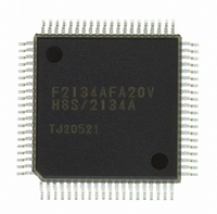
Manufacturer Part Number
DF2134AFA20V
Description
IC H8S/2100 MCU FLASH 80QFP
Manufacturer
Renesas Electronics America
Series
H8® H8S/2100r
Datasheets
1.HEWH8E10A.pdf
(19 pages)
2.D12312SVTE25V.pdf
(341 pages)
3.DF2134AFA20V.pdf
(1063 pages)
Specifications of DF2134AFA20V
Core Processor
H8S/2000
Core Size
16-Bit
Speed
20MHz
Connectivity
IrDA, SCI
Peripherals
POR, PWM, WDT
Number Of I /o
58
Program Memory Size
128KB (128K x 8)
Program Memory Type
FLASH
Ram Size
4K x 8
Voltage - Supply (vcc/vdd)
4 V ~ 5.5 V
Data Converters
A/D 8x10b; D/A 2x8b
Oscillator Type
Internal
Operating Temperature
-20°C ~ 75°C
Package / Case
80-QFP
For Use With
3DK2166 - DEV EVAL KIT H8S/2166
Lead Free Status / RoHS Status
Lead free / RoHS Compliant
Eeprom Size
-
Available stocks
Company
Part Number
Manufacturer
Quantity
Price
Company:

Part Number:
DF2134AFA20V
Manufacturer:
Renesas Electronics America
Quantity:
10 000


Section 13 Timer Connection [H8S/2138 Group]
13.3.2
Clamp Waveform Generation (CL1/CL2/CL3 Signal Generation)
The timer connection facility and TMRX can be used to generate signals with different duty cycles
and rising/falling edges (clamp waveforms) in synchronization with the input signal (IHI signal).
Three clamp waveforms can be generated: the CL1, CL2, and CL3 signals. In addition, the CL4
signal can be generated using TMRY.
The CL1 signal rises simultaneously with the rise of the IHI signal, and when the CL1 signal is
high, the CL2 signal rises simultaneously with the fall of the IHI signal. The fall of both the CL1
and the CL2 signal can be specified by TCORA.
The rise of the CL3 signal can be specified as simultaneous with the sampling of the fall of the IHI
signal using the system clock, and the fall of the CL3 signal can be specified by TCORC. The CL3
signal can also fall when the IHI signal rises.
TCNT in TMRX is set to count internal clock pulses and to be cleared on the rising edge of the
external reset signal (IHI signal).
The value to be used as the CL1 signal pulse width is written in TCORA. Write a value of H'02 or
more in TCORA when internal clock is selected as the TMRX counter clock, and a value or
H'01 or more when /2 is selected. When internal clock is selected, the CL1 signal pulse width
is (TCORA set value + 3 ± 0.5). When the CL2 signal is used, the setting must be made so that
this pulse width is greater than the IHI signal pulse width.
The value to be used as the CL3 signal pulse width is written in TCORC. The TICR register in
TMRX captures the value of TCNT at the inverse of the external reset signal edge (in this case, the
falling edge of the IHI signal). The timing of the fall of the CL3 signal is determined by the sum of
the contents of TICR and TCORC. Caution is required if the rising edge of the IHI signal precedes
the fall timing set by the contents of TCORC, since the IHI signal will cause the CL3 signal to fall.
Examples of TMRX TCR settings are the same as those in table 13.3. The clamp waveform timing
charts are shown in figures 13.3 and 13.4.
Since the rise of the CL1 and CL2 signals is synchronized with the edge of the IHI signal, and
their fall is synchronized with the system clock, the pulse width variation is equivalent to the
resolution of the system clock.
Both the rise and the fall of the CL3 signal are synchronized with the system clock and the pulse
width is fixed, but there is a variation in the phase relationship with the IHI signal equivalent to
the resolution of the system clock.
Rev. 4.00 Jun 06, 2006 page 357 of 1004
REJ09B0301-0400
Related parts for DF2134AFA20V
Image
Part Number
Description
Manufacturer
Datasheet
Request
R

Part Number:
Description:
KIT STARTER FOR M16C/29
Manufacturer:
Renesas Electronics America
Datasheet:

Part Number:
Description:
KIT STARTER FOR R8C/2D
Manufacturer:
Renesas Electronics America
Datasheet:

Part Number:
Description:
R0K33062P STARTER KIT
Manufacturer:
Renesas Electronics America
Datasheet:

Part Number:
Description:
KIT STARTER FOR R8C/23 E8A
Manufacturer:
Renesas Electronics America
Datasheet:

Part Number:
Description:
KIT STARTER FOR R8C/25
Manufacturer:
Renesas Electronics America
Datasheet:

Part Number:
Description:
KIT STARTER H8S2456 SHARPE DSPLY
Manufacturer:
Renesas Electronics America
Datasheet:

Part Number:
Description:
KIT STARTER FOR R8C38C
Manufacturer:
Renesas Electronics America
Datasheet:

Part Number:
Description:
KIT STARTER FOR R8C35C
Manufacturer:
Renesas Electronics America
Datasheet:

Part Number:
Description:
KIT STARTER FOR R8CL3AC+LCD APPS
Manufacturer:
Renesas Electronics America
Datasheet:
Part Number:
Description:
KIT STARTER FOR RX610
Manufacturer:
Renesas Electronics America
Datasheet:

Part Number:
Description:
KIT STARTER FOR R32C/118
Manufacturer:
Renesas Electronics America
Datasheet:

Part Number:
Description:
KIT DEV RSK-R8C/26-29
Manufacturer:
Renesas Electronics America
Datasheet:

Part Number:
Description:
KIT STARTER FOR SH7124
Manufacturer:
Renesas Electronics America
Datasheet:

Part Number:
Description:
KIT STARTER FOR H8SX/1622
Manufacturer:
Renesas Electronics America
Datasheet:

Part Number:
Description:
KIT DEV FOR SH7203
Manufacturer:
Renesas Electronics America
Datasheet: