DF2134AFA20V Renesas Electronics America, DF2134AFA20V Datasheet - Page 51
DF2134AFA20V
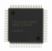
Manufacturer Part Number
DF2134AFA20V
Description
IC H8S/2100 MCU FLASH 80QFP
Manufacturer
Renesas Electronics America
Series
H8® H8S/2100r
Datasheets
1.HEWH8E10A.pdf
(19 pages)
2.D12312SVTE25V.pdf
(341 pages)
3.DF2134AFA20V.pdf
(1063 pages)
Specifications of DF2134AFA20V
Core Processor
H8S/2000
Core Size
16-Bit
Speed
20MHz
Connectivity
IrDA, SCI
Peripherals
POR, PWM, WDT
Number Of I /o
58
Program Memory Size
128KB (128K x 8)
Program Memory Type
FLASH
Ram Size
4K x 8
Voltage - Supply (vcc/vdd)
4 V ~ 5.5 V
Data Converters
A/D 8x10b; D/A 2x8b
Oscillator Type
Internal
Operating Temperature
-20°C ~ 75°C
Package / Case
80-QFP
For Use With
3DK2166 - DEV EVAL KIT H8S/2166
Lead Free Status / RoHS Status
Lead free / RoHS Compliant
Eeprom Size
-
Available stocks
Company
Part Number
Manufacturer
Quantity
Price
Company:

Part Number:
DF2134AFA20V
Manufacturer:
Renesas Electronics America
Quantity:
10 000


Table 13.9
Table 13.10 Meaning of VSYNCO Output in Each Mode......................................................... 368
Section 14 Watchdog Timer (WDT)
Table 14.1
Table 14.2
Section 15 Serial Communication Interface (SCI, IrDA)
Table 15.1
Table 15.2
Table 15.3
Table 15.4
Table 15.5
Table 15.6
Table 15.7
Table 15.8
Table 15.9
Table 15.10 Serial Transfer Formats (Asynchronous Mode) ..................................................... 420
Table 15.11 Receive Errors and Conditions for Occurrence...................................................... 429
Table 15.12 Bit IrCKS2 to IrCKS0 Settings .............................................................................. 449
Table 15.13 SCI Interrupt Sources ............................................................................................. 450
Table 15.14 State of SSR Status Flags and Transfer of Receive Data ...................................... 451
Section 16 I
Table 16.1
Table 16.2
Table 16.3
Table 16.4
Table 16.5
Table 16.6
Table 16.7
Table 16.8
Section 17 Host Interface [H8S/2138 Group]
Table 17.1
Table 17.2
Table 17.3
Table 17.4
Table 17.5
Table 17.6
Table 17.7
Meaning of HSYNCO Output in Each Mode......................................................... 367
WDT Pin ................................................................................................................ 374
WDT Registers....................................................................................................... 374
SCI Pins.................................................................................................................. 390
SCI Registers.......................................................................................................... 391
BRR Settings for Various Bit Rates (Asynchronous Mode) .................................. 406
BRR Settings for Various Bit Rates (Synchronous Mode) .................................... 409
Maximum Bit Rate for Each Frequency (Asynchronous Mode)............................ 411
Maximum Bit Rate with External Clock Input (Asynchronous Mode).................. 412
Maximum Bit Rate with External Clock Input (Synchronous Mode) .................... 413
SMR Settings and Serial Transfer Format Selection.............................................. 418
SMR and SCR Settings and SCI Clock Source Selection ...................................... 418
I
Register Configuration ........................................................................................... 459
Flags and Transfer States ....................................................................................... 474
I
Examples of Operation Using the DTC.................................................................. 499
I
Permissible SCL Rise Time (t
I
Host Interface Registers ......................................................................................... 526
Set/Clear Timing for STR1 Flags........................................................................... 532
Set/Clear Timing for STR2 Flags........................................................................... 535
Host Interface Channel Selection and Pin Operation ............................................. 536
Host Interface Operation ........................................................................................ 537
GA20 (P81) Set/Clear Timing................................................................................ 538
2
Host Interface Input/Output Pins........................................................................... 525
2
2
2
2
C Bus Interface [H8S/2138 Group Option]
C Bus Interface Pins............................................................................................. 458
C Bus Data Format Symbols................................................................................ 487
C Bus Timing (SCL and SDA Output) ................................................................ 507
C Bus Timing (with Maximum Influence of t
Sr
) Values ................................................................. 508
Rev. 4.00 Jun 06, 2006 page xlix of liv
Sr
/t
Sf
)............................................... 509
Related parts for DF2134AFA20V
Image
Part Number
Description
Manufacturer
Datasheet
Request
R

Part Number:
Description:
KIT STARTER FOR M16C/29
Manufacturer:
Renesas Electronics America
Datasheet:

Part Number:
Description:
KIT STARTER FOR R8C/2D
Manufacturer:
Renesas Electronics America
Datasheet:

Part Number:
Description:
R0K33062P STARTER KIT
Manufacturer:
Renesas Electronics America
Datasheet:

Part Number:
Description:
KIT STARTER FOR R8C/23 E8A
Manufacturer:
Renesas Electronics America
Datasheet:

Part Number:
Description:
KIT STARTER FOR R8C/25
Manufacturer:
Renesas Electronics America
Datasheet:

Part Number:
Description:
KIT STARTER H8S2456 SHARPE DSPLY
Manufacturer:
Renesas Electronics America
Datasheet:

Part Number:
Description:
KIT STARTER FOR R8C38C
Manufacturer:
Renesas Electronics America
Datasheet:

Part Number:
Description:
KIT STARTER FOR R8C35C
Manufacturer:
Renesas Electronics America
Datasheet:

Part Number:
Description:
KIT STARTER FOR R8CL3AC+LCD APPS
Manufacturer:
Renesas Electronics America
Datasheet:
Part Number:
Description:
KIT STARTER FOR RX610
Manufacturer:
Renesas Electronics America
Datasheet:

Part Number:
Description:
KIT STARTER FOR R32C/118
Manufacturer:
Renesas Electronics America
Datasheet:

Part Number:
Description:
KIT DEV RSK-R8C/26-29
Manufacturer:
Renesas Electronics America
Datasheet:

Part Number:
Description:
KIT STARTER FOR SH7124
Manufacturer:
Renesas Electronics America
Datasheet:

Part Number:
Description:
KIT STARTER FOR H8SX/1622
Manufacturer:
Renesas Electronics America
Datasheet:

Part Number:
Description:
KIT DEV FOR SH7203
Manufacturer:
Renesas Electronics America
Datasheet: