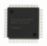
DF2134AFA20V Renesas Electronics America, DF2134AFA20V Datasheet - Page 618

DF2134AFA20V
Manufacturer Part Number
DF2134AFA20V
Description
IC H8S/2100 MCU FLASH 80QFP
Manufacturer
Renesas Electronics America
Series
H8® H8S/2100r
Datasheets
1.HEWH8E10A.pdf
(19 pages)
2.D12312SVTE25V.pdf
(341 pages)
3.DF2134AFA20V.pdf
(1063 pages)
Specifications of DF2134AFA20V
Core Processor
H8S/2000
Core Size
16-Bit
Speed
20MHz
Connectivity
IrDA, SCI
Peripherals
POR, PWM, WDT
Number Of I /o
58
Program Memory Size
128KB (128K x 8)
Program Memory Type
FLASH
Ram Size
4K x 8
Voltage - Supply (vcc/vdd)
4 V ~ 5.5 V
Data Converters
A/D 8x10b; D/A 2x8b
Oscillator Type
Internal
Operating Temperature
-20°C ~ 75°C
Package / Case
80-QFP
For Use With
3DK2166 - DEV EVAL KIT H8S/2166
Lead Free Status / RoHS Status
Lead free / RoHS Compliant
Eeprom Size
-
Available stocks
Company
Part Number
Manufacturer
Quantity
Price
Company:
Part Number:
DF2134AFA20V
Manufacturer:
Renesas Electronics America
Quantity:
10 000
- Current page: 618 of 1063
- Download datasheet (6Mb)
Section 19 A/D Converter
19.4
The A/D converter operates by successive approximations with 10-bit resolution. It has two
operating modes: single mode and scan mode.
19.4.1
Single mode is selected when A/D conversion is to be performed on a single channel only. A/D
conversion is started when the ADST bit is set to 1 by software, or by external trigger input. The
ADST bit remains set to 1 during A/D conversion, and is automatically cleared to 0 when
conversion ends.
On completion of conversion, the ADF flag is set to 1. If the ADIE bit is set to 1 at this time, an
ADI interrupt request is generated. The ADF flag is cleared by writing 0 after reading ADCSR.
When the operating mode or analog input channel must be changed during analog conversion, to
prevent incorrect operation, first clear the ADST bit to 0 in ADCSR to halt A/D conversion. After
making the necessary changes, set the ADST bit to 1 to start A/D conversion again. The ADST bit
can be set at the same time as the operating mode or input channel is changed.
Typical operations when channel 1 (AN1) is selected in single mode are described next. Figure
19.3 shows a timing diagram for this example.
1. Single mode is selected (SCAN = 0), input channel AN1 is selected (CH1 = 0, CH0 = 1), the
2. When A/D conversion is completed, the result is transferred to ADDRB. At the same time the
3. Since ADF = 1 and ADIE = 1, an ADI interrupt is requested.
4. The A/D interrupt handling routine starts.
5. The routine reads ADCSR, then writes 0 to the ADF flag.
6. The routine reads and processes the conversion result (ADDRB).
7. Execution of the A/D interrupt handling routine ends. After that, if the ADST bit is set to 1,
Rev. 4.00 Jun 06, 2006 page 562 of 1004
REJ09B0301-0400
A/D interrupt is enabled (ADIE = 1), and A/D conversion is started (ADST = 1).
ADF flag is set to 1, the ADST bit is cleared to 0, and the A/D converter becomes idle.
A/D conversion starts again and steps 2 to 7 are repeated.
Operation
Single Mode (SCAN = 0)
Related parts for DF2134AFA20V
Image
Part Number
Description
Manufacturer
Datasheet
Request
R

Part Number:
Description:
KIT STARTER FOR M16C/29
Manufacturer:
Renesas Electronics America
Datasheet:

Part Number:
Description:
KIT STARTER FOR R8C/2D
Manufacturer:
Renesas Electronics America
Datasheet:

Part Number:
Description:
R0K33062P STARTER KIT
Manufacturer:
Renesas Electronics America
Datasheet:

Part Number:
Description:
KIT STARTER FOR R8C/23 E8A
Manufacturer:
Renesas Electronics America
Datasheet:

Part Number:
Description:
KIT STARTER FOR R8C/25
Manufacturer:
Renesas Electronics America
Datasheet:

Part Number:
Description:
KIT STARTER H8S2456 SHARPE DSPLY
Manufacturer:
Renesas Electronics America
Datasheet:

Part Number:
Description:
KIT STARTER FOR R8C38C
Manufacturer:
Renesas Electronics America
Datasheet:

Part Number:
Description:
KIT STARTER FOR R8C35C
Manufacturer:
Renesas Electronics America
Datasheet:

Part Number:
Description:
KIT STARTER FOR R8CL3AC+LCD APPS
Manufacturer:
Renesas Electronics America
Datasheet:

Part Number:
Description:
KIT STARTER FOR RX610
Manufacturer:
Renesas Electronics America
Datasheet:

Part Number:
Description:
KIT STARTER FOR R32C/118
Manufacturer:
Renesas Electronics America
Datasheet:

Part Number:
Description:
KIT DEV RSK-R8C/26-29
Manufacturer:
Renesas Electronics America
Datasheet:

Part Number:
Description:
KIT STARTER FOR SH7124
Manufacturer:
Renesas Electronics America
Datasheet:

Part Number:
Description:
KIT STARTER FOR H8SX/1622
Manufacturer:
Renesas Electronics America
Datasheet:

Part Number:
Description:
KIT DEV FOR SH7203
Manufacturer:
Renesas Electronics America
Datasheet:


