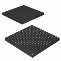
AT91SAM9M10-CU Atmel, AT91SAM9M10-CU Datasheet - Page 1053

AT91SAM9M10-CU
Manufacturer Part Number
AT91SAM9M10-CU
Description
IC MCU 16/32BIT ARM9 324TFBGA
Manufacturer
Atmel
Series
AT91SAMr
Specifications of AT91SAM9M10-CU
Core Processor
ARM9
Core Size
16/32-Bit
Speed
400MHz
Connectivity
EBI/EMI, Ethernet, I²C, SPI, SSC, UART/USART, USB
Peripherals
AC'97, DMA, LCD, POR, PWM, WDT
Number Of I /o
160
Program Memory Size
64KB (64K x 8)
Program Memory Type
ROM
Ram Size
128K x 8
Voltage - Supply (vcc/vdd)
0.9 V ~ 1.1 V
Data Converters
A/D 8x10b
Oscillator Type
Internal
Operating Temperature
-40°C ~ 85°C
Package / Case
324-TFBGA
Processor Series
AT91SAMx
Core
ARM926EJ-S
Data Bus Width
32 bit
Data Ram Size
32 KB
Interface Type
2-Wire, SPI, USART
Maximum Clock Frequency
133 MHz
Number Of Programmable I/os
5
Number Of Timers
2 x 16 bit
Operating Supply Voltage
1.65 V to 3.6 V
Maximum Operating Temperature
+ 85 C
Mounting Style
SMD/SMT
3rd Party Development Tools
JTRACE-ARM-2M, MDK-ARM, RL-ARM, ULINK2
Development Tools By Supplier
AT91SAM-ICE, AT91-ISP, AT91SAM9M10-G45-EK
Controller Family/series
AT91
No. Of I/o's
160
Ram Memory Size
64KB
Cpu Speed
400MHz
No. Of Timers
2
Rohs Compliant
Yes
Cpu Family
AT91
Device Core
ARM926EJ-S
Device Core Size
32b
Frequency (max)
400MHz
Total Internal Ram Size
64KB
# I/os (max)
160
Number Of Timers - General Purpose
7
Operating Supply Voltage (typ)
1.8/2.5/3.3V
Operating Supply Voltage (max)
1.1/1.95/3.6V
Operating Supply Voltage (min)
0.9/1.65/1.8/3V
On-chip Adc
8-chx10-bit
Instruction Set Architecture
RISC
Operating Temp Range
-40C to 85C
Operating Temperature Classification
Industrial
Mounting
Surface Mount
Pin Count
324
Package Type
TFBGA
Lead Free Status / RoHS Status
Lead free / RoHS Compliant
Eeprom Size
-
Lead Free Status / Rohs Status
Lead free / RoHS Compliant
Available stocks
Company
Part Number
Manufacturer
Quantity
Price
Company:
Part Number:
AT91SAM9M10-CU
Manufacturer:
Atmel
Quantity:
996
- Current page: 1053 of 1404
- Download datasheet (22Mb)
43.7.3
Figure 43-4. Logical Channel Assignment
1053
(Controller Output)
(Codec output)
AT91SAM9M10
AC97 Controller Channel Organization
AC97RX
AC97FS
AC97TX
Slot #
AC97C_ICA = 0x0000_0009
AC97C_OCA = 0x0000_0209
TAG
TAG
0
The AC97 Controller features a Codec channel and 2 logical channels: Channel A, Channel B.
The Codec channel controls AC97 Codec registers, it enables write and read configuration val-
ues in order to bring the AC97 Codec to an operating state. The Codec channel always runs slot
1 and slot 2 exclusively, in both input and output directions.
Channel A, Channel B transfer data to/from AC97 codec. All audio samples and modem data
must transit by these 2 channels. However, Channels A and B are connected to PDC channels
thus making it suitable for audio streaming applications.
Each slot of the input or the output frame that belongs to this range [3 to 12] can be operated by
Channel A or Channel B . The slot to channel assignment is configured by two registers:
The AC97 Controller Input Channel Assignment Register (AC97C_ICA) configures the input slot
to channel assignment. The AC97 Controller Output Channel Assignment Register
(AC97C_OCA) configures the output slot to channel assignment.
A slot can be left unassigned to a channel by the AC97 Controller. Slots 0, 1,and 2 cannot be
assigned to Channel A or to Channel Bthrough the AC97C_OCA and AC97C_ICA Registers.
The width of sample data, that transit via the Channel varies and can take one of these values;
10, 16, 18 or 20 bits.
STATUS
• AC97 Controller Input Channel Assignment Register (AC97C_ICA)
• AC97 Controller Output Channel Assignment Register (AC97C_OCA)
ADDR
ADDR
CMD
Codec Channel
1
Codec Channel
STATUS
DATA
DATA
CMD
2
3
L Front
LEFT
PCM
PCM
Channel A
Channel A
R Front
RIGHT
4
PCM
PCM
LINE 1
LINE 1
5
DAC
DAC
6
Center
PCM
PCM
MIC
L SURR
RSVED
7
PCM
R SURR
RSVED
PCM
8
RSVED
PCM
9
LFE
LINE 2
LINE 2
10
ADC
DAC
6355B–ATARM–21-Jun-10
11
HSET
HSET
ADC
DAC
STATUS
12
CTRL
IO
IO
Related parts for AT91SAM9M10-CU
Image
Part Number
Description
Manufacturer
Datasheet
Request
R

Part Number:
Description:
MCU, MPU & DSP Development Tools KICKSTART KIT FOR AT91SAM9 PLUS
Manufacturer:
IAR Systems

Part Number:
Description:
DEV KIT FOR AVR/AVR32
Manufacturer:
Atmel
Datasheet:

Part Number:
Description:
INTERVAL AND WIPE/WASH WIPER CONTROL IC WITH DELAY
Manufacturer:
ATMEL Corporation
Datasheet:

Part Number:
Description:
Low-Voltage Voice-Switched IC for Hands-Free Operation
Manufacturer:
ATMEL Corporation
Datasheet:

Part Number:
Description:
MONOLITHIC INTEGRATED FEATUREPHONE CIRCUIT
Manufacturer:
ATMEL Corporation
Datasheet:

Part Number:
Description:
AM-FM Receiver IC U4255BM-M
Manufacturer:
ATMEL Corporation
Datasheet:

Part Number:
Description:
Monolithic Integrated Feature Phone Circuit
Manufacturer:
ATMEL Corporation
Datasheet:

Part Number:
Description:
Multistandard Video-IF and Quasi Parallel Sound Processing
Manufacturer:
ATMEL Corporation
Datasheet:

Part Number:
Description:
High-performance EE PLD
Manufacturer:
ATMEL Corporation
Datasheet:

Part Number:
Description:
8-bit Flash Microcontroller
Manufacturer:
ATMEL Corporation
Datasheet:

Part Number:
Description:
2-Wire Serial EEPROM
Manufacturer:
ATMEL Corporation
Datasheet:


