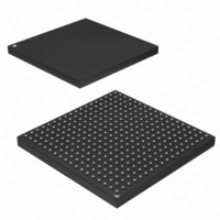
AT91SAM9M10-CU Atmel, AT91SAM9M10-CU Datasheet - Page 460

AT91SAM9M10-CU
Manufacturer Part Number
AT91SAM9M10-CU
Description
IC MCU 16/32BIT ARM9 324TFBGA
Manufacturer
Atmel
Series
AT91SAMr
Specifications of AT91SAM9M10-CU
Core Processor
ARM9
Core Size
16/32-Bit
Speed
400MHz
Connectivity
EBI/EMI, Ethernet, I²C, SPI, SSC, UART/USART, USB
Peripherals
AC'97, DMA, LCD, POR, PWM, WDT
Number Of I /o
160
Program Memory Size
64KB (64K x 8)
Program Memory Type
ROM
Ram Size
128K x 8
Voltage - Supply (vcc/vdd)
0.9 V ~ 1.1 V
Data Converters
A/D 8x10b
Oscillator Type
Internal
Operating Temperature
-40°C ~ 85°C
Package / Case
324-TFBGA
Processor Series
AT91SAMx
Core
ARM926EJ-S
Data Bus Width
32 bit
Data Ram Size
32 KB
Interface Type
2-Wire, SPI, USART
Maximum Clock Frequency
133 MHz
Number Of Programmable I/os
5
Number Of Timers
2 x 16 bit
Operating Supply Voltage
1.65 V to 3.6 V
Maximum Operating Temperature
+ 85 C
Mounting Style
SMD/SMT
3rd Party Development Tools
JTRACE-ARM-2M, MDK-ARM, RL-ARM, ULINK2
Development Tools By Supplier
AT91SAM-ICE, AT91-ISP, AT91SAM9M10-G45-EK
Controller Family/series
AT91
No. Of I/o's
160
Ram Memory Size
64KB
Cpu Speed
400MHz
No. Of Timers
2
Rohs Compliant
Yes
Cpu Family
AT91
Device Core
ARM926EJ-S
Device Core Size
32b
Frequency (max)
400MHz
Total Internal Ram Size
64KB
# I/os (max)
160
Number Of Timers - General Purpose
7
Operating Supply Voltage (typ)
1.8/2.5/3.3V
Operating Supply Voltage (max)
1.1/1.95/3.6V
Operating Supply Voltage (min)
0.9/1.65/1.8/3V
On-chip Adc
8-chx10-bit
Instruction Set Architecture
RISC
Operating Temp Range
-40C to 85C
Operating Temperature Classification
Industrial
Mounting
Surface Mount
Pin Count
324
Package Type
TFBGA
Lead Free Status / RoHS Status
Lead free / RoHS Compliant
Eeprom Size
-
Lead Free Status / Rohs Status
Lead free / RoHS Compliant
Available stocks
Company
Part Number
Manufacturer
Quantity
Price
Company:
Part Number:
AT91SAM9M10-CU
Manufacturer:
Atmel
Quantity:
996
- Current page: 460 of 1404
- Download datasheet (22Mb)
Figure 30-5. Input Glitch Filter Timing
30.4.10
Figure 30-6. Input Change Interrupt Timings
30.4.11
460
if PIO_IFSR = 0
if PIO_IFSR = 1
Read PIO_ISR
PIO_PDSR
PIO_PDSR
Pin Level
Pin Level
PIO_ISR
AT91SAM9M10
MCK
Input Change Interrupt
MCK
Write Protected Registers
The PIO Controller can be programmed to generate an interrupt when it detects an input change
on an I/O line. The Input Change Interrupt is controlled by writing PIO_IER (Interrupt Enable
Register) and PIO_IDR (Interrupt Disable Register), which respectively enable and disable the
input change interrupt by setting and clearing the corresponding bit in PIO_IMR (Interrupt Mask
Register). As Input change detection is possible only by comparing two successive samplings of
the input of the I/O line, the PIO Controller clock must be enabled. The Input Change Interrupt is
available, regardless of the configuration of the I/O line, i.e. configured as an input only, con-
trolled by the PIO Controller or assigned to a peripheral function.
When an input change is detected on an I/O line, the corresponding bit in PIO_ISR (Interrupt
Status Register) is set. If the corresponding bit in PIO_IMR is set, the PIO Controller interrupt
line is asserted. The interrupt signals of the thirty-two channels are ORed-wired together to gen-
erate a single interrupt signal to the Advanced Interrupt Controller.
When the software reads PIO_ISR, all the interrupts are automatically cleared. This signifies that
all the interrupts that are pending when PIO_ISR is read must be handled.
To prevent any single software error that may corrupt the PIO behavior, the registers listed
below can be write-protected by setting the WPEN bit in the PIO Write Protect Mode Register
(PIO_WPMR).
1 cycle
1 cycle
APB Access
up to 1.5 cycles
1 cycle
up to 2.5 cycles
2 cycles
APB Access
6355B–ATARM–21-Jun-10
up to 2 cycles
1 cycle
1 cycle
Related parts for AT91SAM9M10-CU
Image
Part Number
Description
Manufacturer
Datasheet
Request
R

Part Number:
Description:
MCU, MPU & DSP Development Tools KICKSTART KIT FOR AT91SAM9 PLUS
Manufacturer:
IAR Systems

Part Number:
Description:
DEV KIT FOR AVR/AVR32
Manufacturer:
Atmel
Datasheet:

Part Number:
Description:
INTERVAL AND WIPE/WASH WIPER CONTROL IC WITH DELAY
Manufacturer:
ATMEL Corporation
Datasheet:

Part Number:
Description:
Low-Voltage Voice-Switched IC for Hands-Free Operation
Manufacturer:
ATMEL Corporation
Datasheet:

Part Number:
Description:
MONOLITHIC INTEGRATED FEATUREPHONE CIRCUIT
Manufacturer:
ATMEL Corporation
Datasheet:

Part Number:
Description:
AM-FM Receiver IC U4255BM-M
Manufacturer:
ATMEL Corporation
Datasheet:

Part Number:
Description:
Monolithic Integrated Feature Phone Circuit
Manufacturer:
ATMEL Corporation
Datasheet:

Part Number:
Description:
Multistandard Video-IF and Quasi Parallel Sound Processing
Manufacturer:
ATMEL Corporation
Datasheet:

Part Number:
Description:
High-performance EE PLD
Manufacturer:
ATMEL Corporation
Datasheet:

Part Number:
Description:
8-bit Flash Microcontroller
Manufacturer:
ATMEL Corporation
Datasheet:

Part Number:
Description:
2-Wire Serial EEPROM
Manufacturer:
ATMEL Corporation
Datasheet:


