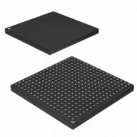
AT91SAM9M10-CU Atmel, AT91SAM9M10-CU Datasheet - Page 252

AT91SAM9M10-CU
Manufacturer Part Number
AT91SAM9M10-CU
Description
IC MCU 16/32BIT ARM9 324TFBGA
Manufacturer
Atmel
Series
AT91SAMr
Specifications of AT91SAM9M10-CU
Core Processor
ARM9
Core Size
16/32-Bit
Speed
400MHz
Connectivity
EBI/EMI, Ethernet, I²C, SPI, SSC, UART/USART, USB
Peripherals
AC'97, DMA, LCD, POR, PWM, WDT
Number Of I /o
160
Program Memory Size
64KB (64K x 8)
Program Memory Type
ROM
Ram Size
128K x 8
Voltage - Supply (vcc/vdd)
0.9 V ~ 1.1 V
Data Converters
A/D 8x10b
Oscillator Type
Internal
Operating Temperature
-40°C ~ 85°C
Package / Case
324-TFBGA
Processor Series
AT91SAMx
Core
ARM926EJ-S
Data Bus Width
32 bit
Data Ram Size
32 KB
Interface Type
2-Wire, SPI, USART
Maximum Clock Frequency
133 MHz
Number Of Programmable I/os
5
Number Of Timers
2 x 16 bit
Operating Supply Voltage
1.65 V to 3.6 V
Maximum Operating Temperature
+ 85 C
Mounting Style
SMD/SMT
3rd Party Development Tools
JTRACE-ARM-2M, MDK-ARM, RL-ARM, ULINK2
Development Tools By Supplier
AT91SAM-ICE, AT91-ISP, AT91SAM9M10-G45-EK
Controller Family/series
AT91
No. Of I/o's
160
Ram Memory Size
64KB
Cpu Speed
400MHz
No. Of Timers
2
Rohs Compliant
Yes
Cpu Family
AT91
Device Core
ARM926EJ-S
Device Core Size
32b
Frequency (max)
400MHz
Total Internal Ram Size
64KB
# I/os (max)
160
Number Of Timers - General Purpose
7
Operating Supply Voltage (typ)
1.8/2.5/3.3V
Operating Supply Voltage (max)
1.1/1.95/3.6V
Operating Supply Voltage (min)
0.9/1.65/1.8/3V
On-chip Adc
8-chx10-bit
Instruction Set Architecture
RISC
Operating Temp Range
-40C to 85C
Operating Temperature Classification
Industrial
Mounting
Surface Mount
Pin Count
324
Package Type
TFBGA
Lead Free Status / RoHS Status
Lead free / RoHS Compliant
Eeprom Size
-
Lead Free Status / Rohs Status
Lead free / RoHS Compliant
Available stocks
Company
Part Number
Manufacturer
Quantity
Price
Company:
Part Number:
AT91SAM9M10-CU
Manufacturer:
Atmel
Quantity:
996
- Current page: 252 of 1404
- Download datasheet (22Mb)
22.4.5
Figure 22-24. Trp and Trcd Timings
252
COMMAND
AT91SAM9M10
Multi-port Functionality
DQS[1:0]
SDCLK
BA[1:0]
DM1:0]
D[15:0]
A[12:0]
NOP
0
3
The SDRAM protocol imposes a check of timings prior to performing a read or a write access,
thus decreasing the performance of systems. An access to SDRAM is performed if banks and
rows are open (or active). To activate a row in a particular bank, it has to de-active the last open
row and open the new row. Two SDRAM commands must be performed to open a bank: Pre-
charge and Active command with respect to Trp timing. Before performing a read or write
command, Trcd timing must checked.
This operation represents a significative loss. (see
The multi-port controller has been designed to mask these timings and thus improve the band-
width of the system.
DDRSDRC is a multi-port controller since four masters can simultaneously reach the controller.
This feature improves the bandwidth of the system because it can detect four requests on the
AHB slave inputs and thus anticipate the commands that follow, PRECHARGE and ACTIVE
commands in bank X during current access in bank Y. This allows Trp and Trcd timings to be
masked (see
were already open. The best condition is met when the four masters work in different banks. In
the case of four simultaneous read accesses, when the four banks and associated rows are
open, the controller reads with a continuous flow and masks the cas latency for each different
access. To allow a continuous flow, the read command must be set at 2 or 3 cycles (cas latency)
before the end of current access. This requires that the scheme of arbitration changes since the
round-robin arbitration cannot be respected. If the controller anticipates a read access, and thus
before the end of current access a master with a high priority arises, then this master will not
serviced.
The arbitration mechanism reduces latency when conflicts occur, i.e., when two or more masters
try to access the SDRAM device at the same time.
PRCHG
NOP
Trp
4 cycles before performing a read command
Figure
ACT
22-25). In the best case, all accesses are done as if the banks and rows
NOP
Trcd
READ
BST
Latency =2
Figure
NOP
22-24).
Da Db
6355B–ATARM–21-Jun-10
Related parts for AT91SAM9M10-CU
Image
Part Number
Description
Manufacturer
Datasheet
Request
R

Part Number:
Description:
MCU, MPU & DSP Development Tools KICKSTART KIT FOR AT91SAM9 PLUS
Manufacturer:
IAR Systems

Part Number:
Description:
DEV KIT FOR AVR/AVR32
Manufacturer:
Atmel
Datasheet:

Part Number:
Description:
INTERVAL AND WIPE/WASH WIPER CONTROL IC WITH DELAY
Manufacturer:
ATMEL Corporation
Datasheet:

Part Number:
Description:
Low-Voltage Voice-Switched IC for Hands-Free Operation
Manufacturer:
ATMEL Corporation
Datasheet:

Part Number:
Description:
MONOLITHIC INTEGRATED FEATUREPHONE CIRCUIT
Manufacturer:
ATMEL Corporation
Datasheet:

Part Number:
Description:
AM-FM Receiver IC U4255BM-M
Manufacturer:
ATMEL Corporation
Datasheet:

Part Number:
Description:
Monolithic Integrated Feature Phone Circuit
Manufacturer:
ATMEL Corporation
Datasheet:

Part Number:
Description:
Multistandard Video-IF and Quasi Parallel Sound Processing
Manufacturer:
ATMEL Corporation
Datasheet:

Part Number:
Description:
High-performance EE PLD
Manufacturer:
ATMEL Corporation
Datasheet:

Part Number:
Description:
8-bit Flash Microcontroller
Manufacturer:
ATMEL Corporation
Datasheet:

Part Number:
Description:
2-Wire Serial EEPROM
Manufacturer:
ATMEL Corporation
Datasheet:


