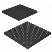
AT91SAM9M10-CU Atmel, AT91SAM9M10-CU Datasheet - Page 565

AT91SAM9M10-CU
Manufacturer Part Number
AT91SAM9M10-CU
Description
IC MCU 16/32BIT ARM9 324TFBGA
Manufacturer
Atmel
Series
AT91SAMr
Specifications of AT91SAM9M10-CU
Core Processor
ARM9
Core Size
16/32-Bit
Speed
400MHz
Connectivity
EBI/EMI, Ethernet, I²C, SPI, SSC, UART/USART, USB
Peripherals
AC'97, DMA, LCD, POR, PWM, WDT
Number Of I /o
160
Program Memory Size
64KB (64K x 8)
Program Memory Type
ROM
Ram Size
128K x 8
Voltage - Supply (vcc/vdd)
0.9 V ~ 1.1 V
Data Converters
A/D 8x10b
Oscillator Type
Internal
Operating Temperature
-40°C ~ 85°C
Package / Case
324-TFBGA
Processor Series
AT91SAMx
Core
ARM926EJ-S
Data Bus Width
32 bit
Data Ram Size
32 KB
Interface Type
2-Wire, SPI, USART
Maximum Clock Frequency
133 MHz
Number Of Programmable I/os
5
Number Of Timers
2 x 16 bit
Operating Supply Voltage
1.65 V to 3.6 V
Maximum Operating Temperature
+ 85 C
Mounting Style
SMD/SMT
3rd Party Development Tools
JTRACE-ARM-2M, MDK-ARM, RL-ARM, ULINK2
Development Tools By Supplier
AT91SAM-ICE, AT91-ISP, AT91SAM9M10-G45-EK
Controller Family/series
AT91
No. Of I/o's
160
Ram Memory Size
64KB
Cpu Speed
400MHz
No. Of Timers
2
Rohs Compliant
Yes
Cpu Family
AT91
Device Core
ARM926EJ-S
Device Core Size
32b
Frequency (max)
400MHz
Total Internal Ram Size
64KB
# I/os (max)
160
Number Of Timers - General Purpose
7
Operating Supply Voltage (typ)
1.8/2.5/3.3V
Operating Supply Voltage (max)
1.1/1.95/3.6V
Operating Supply Voltage (min)
0.9/1.65/1.8/3V
On-chip Adc
8-chx10-bit
Instruction Set Architecture
RISC
Operating Temp Range
-40C to 85C
Operating Temperature Classification
Industrial
Mounting
Surface Mount
Pin Count
324
Package Type
TFBGA
Lead Free Status / RoHS Status
Lead free / RoHS Compliant
Eeprom Size
-
Lead Free Status / Rohs Status
Lead free / RoHS Compliant
Available stocks
Company
Part Number
Manufacturer
Quantity
Price
Company:
Part Number:
AT91SAM9M10-CU
Manufacturer:
Atmel
Quantity:
996
- Current page: 565 of 1404
- Download datasheet (22Mb)
32.7.8.5
Figure 32-40. Header Transmission
6355B–ATARM–21-Jun-10
Write RSTSTA=1
in US_CSR
in US_CSR
Baud Rate
US_LINIR
US_LINIR
in US_CR
TXRDY
LINBK
LINID
Clock
Write
TXD
Header Transmission (Master Node Configuration)
ID
All the LIN Frames start with a header which is sent by the master node and consists of a Synch
Break Field, Synch Field and Identifier Field.
So in Master node configuration, the frame handling starts with the sending of the header.
The header is transmitted as soon as the identifier is written in the LIN Identifier register
(US_LINIR). At this moment the flag TXRDY falls.
The Break Field, the Synch Field and the Identifier Field are sent automatically one after the
other.
The Break Field consists of 13 dominant bits and 1 recessive bit, the Synch Field is the charac-
ter 0x55 and the Identifier corresponds to the character written in the LIN Identifier Register
(US_LINIR). The Identifier parity bits can be automatically computed and sent (see
32.7.8.8).
The flag TXRDY rises when the identifier character is transferred into the Shift Register of the
transmitter.As soon as the Synch Break Field is transmitted, the flag LINBK in the Channel Sta-
tus register (US_CSR) is set to “1”. Likewise, as soon as the Identifier Field is sent, the flag
LINID in the Channel Status register (US_CSR) is set to “1”. These flags are reset by writing the
bit RSTSTA at “1” in the Control register (US_CR).
13 dominant bits (at 0)
Break Field
1 recessive bit
Delimiter
Break
(at 1)
Start
Bit
1
0
Synch Byte = 0x55
1
0
1
0
1
0
Stop
Bit
Start
Bit
ID0
ID1
AT91SAM9M10
ID2
ID3
ID4
ID5
ID6
ID7
Stop
Bit
Section
565
Related parts for AT91SAM9M10-CU
Image
Part Number
Description
Manufacturer
Datasheet
Request
R

Part Number:
Description:
MCU, MPU & DSP Development Tools KICKSTART KIT FOR AT91SAM9 PLUS
Manufacturer:
IAR Systems

Part Number:
Description:
DEV KIT FOR AVR/AVR32
Manufacturer:
Atmel
Datasheet:

Part Number:
Description:
INTERVAL AND WIPE/WASH WIPER CONTROL IC WITH DELAY
Manufacturer:
ATMEL Corporation
Datasheet:

Part Number:
Description:
Low-Voltage Voice-Switched IC for Hands-Free Operation
Manufacturer:
ATMEL Corporation
Datasheet:

Part Number:
Description:
MONOLITHIC INTEGRATED FEATUREPHONE CIRCUIT
Manufacturer:
ATMEL Corporation
Datasheet:

Part Number:
Description:
AM-FM Receiver IC U4255BM-M
Manufacturer:
ATMEL Corporation
Datasheet:

Part Number:
Description:
Monolithic Integrated Feature Phone Circuit
Manufacturer:
ATMEL Corporation
Datasheet:

Part Number:
Description:
Multistandard Video-IF and Quasi Parallel Sound Processing
Manufacturer:
ATMEL Corporation
Datasheet:

Part Number:
Description:
High-performance EE PLD
Manufacturer:
ATMEL Corporation
Datasheet:

Part Number:
Description:
8-bit Flash Microcontroller
Manufacturer:
ATMEL Corporation
Datasheet:

Part Number:
Description:
2-Wire Serial EEPROM
Manufacturer:
ATMEL Corporation
Datasheet:


