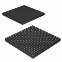
AT91SAM9M10-CU Atmel, AT91SAM9M10-CU Datasheet - Page 44

AT91SAM9M10-CU
Manufacturer Part Number
AT91SAM9M10-CU
Description
IC MCU 16/32BIT ARM9 324TFBGA
Manufacturer
Atmel
Series
AT91SAMr
Specifications of AT91SAM9M10-CU
Core Processor
ARM9
Core Size
16/32-Bit
Speed
400MHz
Connectivity
EBI/EMI, Ethernet, I²C, SPI, SSC, UART/USART, USB
Peripherals
AC'97, DMA, LCD, POR, PWM, WDT
Number Of I /o
160
Program Memory Size
64KB (64K x 8)
Program Memory Type
ROM
Ram Size
128K x 8
Voltage - Supply (vcc/vdd)
0.9 V ~ 1.1 V
Data Converters
A/D 8x10b
Oscillator Type
Internal
Operating Temperature
-40°C ~ 85°C
Package / Case
324-TFBGA
Processor Series
AT91SAMx
Core
ARM926EJ-S
Data Bus Width
32 bit
Data Ram Size
32 KB
Interface Type
2-Wire, SPI, USART
Maximum Clock Frequency
133 MHz
Number Of Programmable I/os
5
Number Of Timers
2 x 16 bit
Operating Supply Voltage
1.65 V to 3.6 V
Maximum Operating Temperature
+ 85 C
Mounting Style
SMD/SMT
3rd Party Development Tools
JTRACE-ARM-2M, MDK-ARM, RL-ARM, ULINK2
Development Tools By Supplier
AT91SAM-ICE, AT91-ISP, AT91SAM9M10-G45-EK
Controller Family/series
AT91
No. Of I/o's
160
Ram Memory Size
64KB
Cpu Speed
400MHz
No. Of Timers
2
Rohs Compliant
Yes
Cpu Family
AT91
Device Core
ARM926EJ-S
Device Core Size
32b
Frequency (max)
400MHz
Total Internal Ram Size
64KB
# I/os (max)
160
Number Of Timers - General Purpose
7
Operating Supply Voltage (typ)
1.8/2.5/3.3V
Operating Supply Voltage (max)
1.1/1.95/3.6V
Operating Supply Voltage (min)
0.9/1.65/1.8/3V
On-chip Adc
8-chx10-bit
Instruction Set Architecture
RISC
Operating Temp Range
-40C to 85C
Operating Temperature Classification
Industrial
Mounting
Surface Mount
Pin Count
324
Package Type
TFBGA
Lead Free Status / RoHS Status
Lead free / RoHS Compliant
Eeprom Size
-
Lead Free Status / Rohs Status
Lead free / RoHS Compliant
Available stocks
Company
Part Number
Manufacturer
Quantity
Price
Company:
Part Number:
AT91SAM9M10-CU
Manufacturer:
Atmel
Quantity:
996
- Current page: 44 of 1404
- Download datasheet (22Mb)
9.6
9.6.1
9.6.2
44
Memory Management Unit (MMU)
AT91SAM9M10
Access Control Logic
Translation Look-aside Buffer (TLB)
The ARM926EJ-S processor implements an enhanced ARM architecture v5 MMU to provide vir-
tual memory features required by operating systems like Symbian OS
Linux
physical address translations.
The Virtual Address generated by the CPU core is converted to a Modified Virtual Address
(MVA) by the FCSE (Fast Context Switch Extension) using the value in CP15 register13. The
MMU translates modified virtual addresses to physical addresses by using a single, two-level
page table set stored in physical memory. Each entry in the set contains the access permissions
and the physical address that correspond to the virtual address.
The first level translation tables contain 4096 entries indexed by bits [31:20] of the MVA. These
entries contain a pointer to either a 1 MB section of physical memory along with attribute infor-
mation (access permissions, domain, etc.) or an entry in the second level translation tables;
coarse table and fine table.
The second level translation tables contain two subtables, coarse table and fine table. An entry
in the coarse table contains a pointer to both large pages and small pages along with access
permissions. An entry in the fine table contains a pointer to large, small and tiny pages.
Table 7 shows the different attributes of each page in the physical memory.
Table 9-6.
The MMU consists of:
The access control logic controls access information for every entry in the translation table. The
access control logic checks two pieces of access information: domain and access permissions.
The domain is the primary access control mechanism for a memory region; there are 16 of them.
It defines the conditions necessary for an access to proceed. The domain determines whether
the access permissions are used to qualify the access or whether they should be ignored.
The second access control mechanism is access permissions that are defined for sections and
for large, small and tiny pages. Sections and tiny pages have a single set of access permissions
whereas large and small pages can be associated with 4 sets of access permissions, one for
each subpage (quarter of a page).
The Translation Look-aside Buffer (TLB) caches translated entries and thus avoids going
through the translation process every time. When the TLB contains an entry for the MVA (Modi-
Mapping Name
Section
Large Page
Small Page
Tiny Page
• Access control logic
• Translation Look-aside Buffer (TLB)
• Translation table walk hardware
®
. These virtual memory features are memory access permission controls and virtual to
Mapping Details
4K bytes
1K byte
Mapping Size
1M byte
64K bytes
Access Permission By
Section
4 separated subpages
4 separated subpages
Tiny Page
®
, Windows CE
-
-
Subpage Size
16K bytes
1K byte
6355B–ATARM–21-Jun-10
®
, and
Related parts for AT91SAM9M10-CU
Image
Part Number
Description
Manufacturer
Datasheet
Request
R

Part Number:
Description:
MCU, MPU & DSP Development Tools KICKSTART KIT FOR AT91SAM9 PLUS
Manufacturer:
IAR Systems

Part Number:
Description:
DEV KIT FOR AVR/AVR32
Manufacturer:
Atmel
Datasheet:

Part Number:
Description:
INTERVAL AND WIPE/WASH WIPER CONTROL IC WITH DELAY
Manufacturer:
ATMEL Corporation
Datasheet:

Part Number:
Description:
Low-Voltage Voice-Switched IC for Hands-Free Operation
Manufacturer:
ATMEL Corporation
Datasheet:

Part Number:
Description:
MONOLITHIC INTEGRATED FEATUREPHONE CIRCUIT
Manufacturer:
ATMEL Corporation
Datasheet:

Part Number:
Description:
AM-FM Receiver IC U4255BM-M
Manufacturer:
ATMEL Corporation
Datasheet:

Part Number:
Description:
Monolithic Integrated Feature Phone Circuit
Manufacturer:
ATMEL Corporation
Datasheet:

Part Number:
Description:
Multistandard Video-IF and Quasi Parallel Sound Processing
Manufacturer:
ATMEL Corporation
Datasheet:

Part Number:
Description:
High-performance EE PLD
Manufacturer:
ATMEL Corporation
Datasheet:

Part Number:
Description:
8-bit Flash Microcontroller
Manufacturer:
ATMEL Corporation
Datasheet:

Part Number:
Description:
2-Wire Serial EEPROM
Manufacturer:
ATMEL Corporation
Datasheet:


