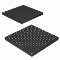
AT91SAM9M10-CU Atmel, AT91SAM9M10-CU Datasheet - Page 34

AT91SAM9M10-CU
Manufacturer Part Number
AT91SAM9M10-CU
Description
IC MCU 16/32BIT ARM9 324TFBGA
Manufacturer
Atmel
Series
AT91SAMr
Specifications of AT91SAM9M10-CU
Core Processor
ARM9
Core Size
16/32-Bit
Speed
400MHz
Connectivity
EBI/EMI, Ethernet, I²C, SPI, SSC, UART/USART, USB
Peripherals
AC'97, DMA, LCD, POR, PWM, WDT
Number Of I /o
160
Program Memory Size
64KB (64K x 8)
Program Memory Type
ROM
Ram Size
128K x 8
Voltage - Supply (vcc/vdd)
0.9 V ~ 1.1 V
Data Converters
A/D 8x10b
Oscillator Type
Internal
Operating Temperature
-40°C ~ 85°C
Package / Case
324-TFBGA
Processor Series
AT91SAMx
Core
ARM926EJ-S
Data Bus Width
32 bit
Data Ram Size
32 KB
Interface Type
2-Wire, SPI, USART
Maximum Clock Frequency
133 MHz
Number Of Programmable I/os
5
Number Of Timers
2 x 16 bit
Operating Supply Voltage
1.65 V to 3.6 V
Maximum Operating Temperature
+ 85 C
Mounting Style
SMD/SMT
3rd Party Development Tools
JTRACE-ARM-2M, MDK-ARM, RL-ARM, ULINK2
Development Tools By Supplier
AT91SAM-ICE, AT91-ISP, AT91SAM9M10-G45-EK
Controller Family/series
AT91
No. Of I/o's
160
Ram Memory Size
64KB
Cpu Speed
400MHz
No. Of Timers
2
Rohs Compliant
Yes
Cpu Family
AT91
Device Core
ARM926EJ-S
Device Core Size
32b
Frequency (max)
400MHz
Total Internal Ram Size
64KB
# I/os (max)
160
Number Of Timers - General Purpose
7
Operating Supply Voltage (typ)
1.8/2.5/3.3V
Operating Supply Voltage (max)
1.1/1.95/3.6V
Operating Supply Voltage (min)
0.9/1.65/1.8/3V
On-chip Adc
8-chx10-bit
Instruction Set Architecture
RISC
Operating Temp Range
-40C to 85C
Operating Temperature Classification
Industrial
Mounting
Surface Mount
Pin Count
324
Package Type
TFBGA
Lead Free Status / RoHS Status
Lead free / RoHS Compliant
Eeprom Size
-
Lead Free Status / Rohs Status
Lead free / RoHS Compliant
Available stocks
Company
Part Number
Manufacturer
Quantity
Price
Company:
Part Number:
AT91SAM9M10-CU
Manufacturer:
Atmel
Quantity:
996
- Current page: 34 of 1404
- Download datasheet (22Mb)
9.4
9.4.1
9.4.2
9.4.3
9.4.4
9.4.5
34
ARM9EJ-S Processor
AT91SAM9M10
ARM9EJ-S Operating States
Switching State
Instruction Pipelines
Memory Access
Jazelle Technology
The ARM9EJ-S processor can operate in three different states, each with a specific instruction
set:
In Jazelle state, all instruction Fetches are in words.
The operating state of the ARM9EJ-S core can be switched between:
All exceptions are entered, handled and exited in ARM state. If an exception occurs in Thumb or
Jazelle states, the processor reverts to ARM state. The transition back to Thumb or Jazelle
states occurs automatically on return from the exception handler.
The ARM9EJ-S core uses two kinds of pipelines to increase the speed of the flow of instructions
to the processor.
A five-stage (five clock cycles) pipeline is used for ARM and Thumb states. It consists of Fetch,
Decode, Execute, Memory and Writeback stages.
A six-stage (six clock cycles) pipeline is used for Jazelle state It consists of Fetch,
Jazelle/Decode (two clock cycles), Execute, Memory and Writeback stages.
The ARM9EJ-S core supports byte (8-bit), half-word (16-bit) and word (32-bit) access. Words
must be aligned to four-byte boundaries, half-words must be aligned to two-byte boundaries and
bytes can be placed on any byte boundary.
Because of the nature of the pipelines, it is possible for a value to be required for use before it
has been placed in the register bank by the actions of an earlier instruction. The ARM9EJ-S con-
trol logic automatically detects these cases and stalls the core or forward data.
The Jazelle technology enables direct and efficient execution of Java byte codes on ARM pro-
cessors, providing high performance for the next generation of Java-powered wireless and
embedded devices.
The new Java feature of ARM9EJ-S can be described as a hardware emulation of a JVM (Java
Virtual Machine). Java mode will appear as another state: instead of executing ARM or Thumb
instructions, it executes Java byte codes. The Java byte code decoder logic implemented in
ARM9EJ-S decodes 95% of executed byte codes and turns them into ARM instructions without
any overhead, while less frequently used byte codes are broken down into optimized sequences
of ARM instructions. The hardware/software split is invisible to the programmer, invisible to the
application and invisible to the operating system. All existing ARM registers are re-used in
Jazelle state and all registers then have particular functions in this mode.
• ARM state: 32-bit, word-aligned ARM instructions.
• THUMB state: 16-bit, halfword-aligned Thumb instructions.
• Jazelle state: variable length, byte-aligned Jazelle instructions.
• ARM state and THUMB state using the BX and BLX instructions, and loads to the PC
• ARM state and Jazelle state using the BXJ instruction
6355B–ATARM–21-Jun-10
Related parts for AT91SAM9M10-CU
Image
Part Number
Description
Manufacturer
Datasheet
Request
R

Part Number:
Description:
MCU, MPU & DSP Development Tools KICKSTART KIT FOR AT91SAM9 PLUS
Manufacturer:
IAR Systems

Part Number:
Description:
DEV KIT FOR AVR/AVR32
Manufacturer:
Atmel
Datasheet:

Part Number:
Description:
INTERVAL AND WIPE/WASH WIPER CONTROL IC WITH DELAY
Manufacturer:
ATMEL Corporation
Datasheet:

Part Number:
Description:
Low-Voltage Voice-Switched IC for Hands-Free Operation
Manufacturer:
ATMEL Corporation
Datasheet:

Part Number:
Description:
MONOLITHIC INTEGRATED FEATUREPHONE CIRCUIT
Manufacturer:
ATMEL Corporation
Datasheet:

Part Number:
Description:
AM-FM Receiver IC U4255BM-M
Manufacturer:
ATMEL Corporation
Datasheet:

Part Number:
Description:
Monolithic Integrated Feature Phone Circuit
Manufacturer:
ATMEL Corporation
Datasheet:

Part Number:
Description:
Multistandard Video-IF and Quasi Parallel Sound Processing
Manufacturer:
ATMEL Corporation
Datasheet:

Part Number:
Description:
High-performance EE PLD
Manufacturer:
ATMEL Corporation
Datasheet:

Part Number:
Description:
8-bit Flash Microcontroller
Manufacturer:
ATMEL Corporation
Datasheet:

Part Number:
Description:
2-Wire Serial EEPROM
Manufacturer:
ATMEL Corporation
Datasheet:


