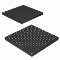
AT91SAM9M10-CU Atmel, AT91SAM9M10-CU Datasheet - Page 410

AT91SAM9M10-CU
Manufacturer Part Number
AT91SAM9M10-CU
Description
IC MCU 16/32BIT ARM9 324TFBGA
Manufacturer
Atmel
Series
AT91SAMr
Specifications of AT91SAM9M10-CU
Core Processor
ARM9
Core Size
16/32-Bit
Speed
400MHz
Connectivity
EBI/EMI, Ethernet, I²C, SPI, SSC, UART/USART, USB
Peripherals
AC'97, DMA, LCD, POR, PWM, WDT
Number Of I /o
160
Program Memory Size
64KB (64K x 8)
Program Memory Type
ROM
Ram Size
128K x 8
Voltage - Supply (vcc/vdd)
0.9 V ~ 1.1 V
Data Converters
A/D 8x10b
Oscillator Type
Internal
Operating Temperature
-40°C ~ 85°C
Package / Case
324-TFBGA
Processor Series
AT91SAMx
Core
ARM926EJ-S
Data Bus Width
32 bit
Data Ram Size
32 KB
Interface Type
2-Wire, SPI, USART
Maximum Clock Frequency
133 MHz
Number Of Programmable I/os
5
Number Of Timers
2 x 16 bit
Operating Supply Voltage
1.65 V to 3.6 V
Maximum Operating Temperature
+ 85 C
Mounting Style
SMD/SMT
3rd Party Development Tools
JTRACE-ARM-2M, MDK-ARM, RL-ARM, ULINK2
Development Tools By Supplier
AT91SAM-ICE, AT91-ISP, AT91SAM9M10-G45-EK
Controller Family/series
AT91
No. Of I/o's
160
Ram Memory Size
64KB
Cpu Speed
400MHz
No. Of Timers
2
Rohs Compliant
Yes
Cpu Family
AT91
Device Core
ARM926EJ-S
Device Core Size
32b
Frequency (max)
400MHz
Total Internal Ram Size
64KB
# I/os (max)
160
Number Of Timers - General Purpose
7
Operating Supply Voltage (typ)
1.8/2.5/3.3V
Operating Supply Voltage (max)
1.1/1.95/3.6V
Operating Supply Voltage (min)
0.9/1.65/1.8/3V
On-chip Adc
8-chx10-bit
Instruction Set Architecture
RISC
Operating Temp Range
-40C to 85C
Operating Temperature Classification
Industrial
Mounting
Surface Mount
Pin Count
324
Package Type
TFBGA
Lead Free Status / RoHS Status
Lead free / RoHS Compliant
Eeprom Size
-
Lead Free Status / Rohs Status
Lead free / RoHS Compliant
Available stocks
Company
Part Number
Manufacturer
Quantity
Price
Company:
Part Number:
AT91SAM9M10-CU
Manufacturer:
Atmel
Quantity:
996
- Current page: 410 of 1404
- Download datasheet (22Mb)
28.7.3.7
28.7.3.8
410
AT91SAM9M10
Transfer Size
SPI Direct Access Memory Controller (DMAC)
ever the SPI still controls the number of bits (8 to16) to be transferred through MISO and MOSI
lines with the chip select configuration registers. This is not the optimal means in term of mem-
ory size for the buffers, but it provides a very effective means to exchange data with several
peripherals without any intervention of the processor.
Depending on the data size to transmit, from 8 to 16 bits, the PDC manages automatically the
type of pointer's size it has to point to. The PDC will perform the following transfer size depend-
ing on the mode and number of bits per data.
Fixed Mode:
Variable Mode:
In variable Mode, PDC Pointer Address = Address +4 bytes and PDC Counter = Counter - 1 for
8 to 16-bit transfer size. When using the PDC, the TDRE and RDRF flags are handled by the
PDC, thus the user’s application does not have to check those bits. Only End of RX Buffer
(ENDRX), End of TX Buffer (ENDTX), Buffer Full (RXBUFF), TX Buffer Empty (TXBUFE) are
significant. For further details about the Peripheral DMA Controller and user interface, refer to
the PDC section of the product datasheet.
In both fixed and variable mode the Direct Memory Access Controller (DMAC) can be used to
reduce processor overhead.
The Fixed Peripheral Selection allows buffer transfers with a single peripheral. Using the DMAC
is an optimal means, as the size of the data transfer between the memory and the SPI is either 8
bits or 16 bits. However, changing the peripheral selection requires the Mode Register to be
reprogrammed.
The Variable Peripheral Selection allows buffer transfers with multiple peripherals without repro-
gramming the Mode Register. Data written in SPI_TDR is 32 bits wide and defines the real data
to be transmitted and the peripheral it is destined to. Using the DMAC in this mode requires 32-
bit wide buffers, with the data in the LSBs and the PCS and LASTXFER fields in the MSBs, how-
ever the SPI still controls the number of bits (8 to16) to be transferred through MISO and MOSI
lines with the chip select configuration registers. This is not the optimal means in term of mem-
ory size for the buffers, but it provides a very effective means to exchange data with several
peripherals without any intervention of the processor.
• 8-bit Data:
• 8-bit to 16-bit Data:
Byte transfer,
PDC Pointer Address = Address + 1 byte,
PDC Counter = Counter - 1
2 bytes transfer. n-bit data transfer with don’t care data (MSB) filled with 0’s,
PDC Pointer Address = Address + 2 bytes,
PDC Counter = Counter - 1
6355B–ATARM–21-Jun-10
Related parts for AT91SAM9M10-CU
Image
Part Number
Description
Manufacturer
Datasheet
Request
R

Part Number:
Description:
MCU, MPU & DSP Development Tools KICKSTART KIT FOR AT91SAM9 PLUS
Manufacturer:
IAR Systems

Part Number:
Description:
DEV KIT FOR AVR/AVR32
Manufacturer:
Atmel
Datasheet:

Part Number:
Description:
INTERVAL AND WIPE/WASH WIPER CONTROL IC WITH DELAY
Manufacturer:
ATMEL Corporation
Datasheet:

Part Number:
Description:
Low-Voltage Voice-Switched IC for Hands-Free Operation
Manufacturer:
ATMEL Corporation
Datasheet:

Part Number:
Description:
MONOLITHIC INTEGRATED FEATUREPHONE CIRCUIT
Manufacturer:
ATMEL Corporation
Datasheet:

Part Number:
Description:
AM-FM Receiver IC U4255BM-M
Manufacturer:
ATMEL Corporation
Datasheet:

Part Number:
Description:
Monolithic Integrated Feature Phone Circuit
Manufacturer:
ATMEL Corporation
Datasheet:

Part Number:
Description:
Multistandard Video-IF and Quasi Parallel Sound Processing
Manufacturer:
ATMEL Corporation
Datasheet:

Part Number:
Description:
High-performance EE PLD
Manufacturer:
ATMEL Corporation
Datasheet:

Part Number:
Description:
8-bit Flash Microcontroller
Manufacturer:
ATMEL Corporation
Datasheet:

Part Number:
Description:
2-Wire Serial EEPROM
Manufacturer:
ATMEL Corporation
Datasheet:


