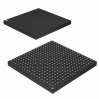
AT91SAM9M10-CU Atmel, AT91SAM9M10-CU Datasheet - Page 18

AT91SAM9M10-CU
Manufacturer Part Number
AT91SAM9M10-CU
Description
IC MCU 16/32BIT ARM9 324TFBGA
Manufacturer
Atmel
Series
AT91SAMr
Specifications of AT91SAM9M10-CU
Core Processor
ARM9
Core Size
16/32-Bit
Speed
400MHz
Connectivity
EBI/EMI, Ethernet, I²C, SPI, SSC, UART/USART, USB
Peripherals
AC'97, DMA, LCD, POR, PWM, WDT
Number Of I /o
160
Program Memory Size
64KB (64K x 8)
Program Memory Type
ROM
Ram Size
128K x 8
Voltage - Supply (vcc/vdd)
0.9 V ~ 1.1 V
Data Converters
A/D 8x10b
Oscillator Type
Internal
Operating Temperature
-40°C ~ 85°C
Package / Case
324-TFBGA
Processor Series
AT91SAMx
Core
ARM926EJ-S
Data Bus Width
32 bit
Data Ram Size
32 KB
Interface Type
2-Wire, SPI, USART
Maximum Clock Frequency
133 MHz
Number Of Programmable I/os
5
Number Of Timers
2 x 16 bit
Operating Supply Voltage
1.65 V to 3.6 V
Maximum Operating Temperature
+ 85 C
Mounting Style
SMD/SMT
3rd Party Development Tools
JTRACE-ARM-2M, MDK-ARM, RL-ARM, ULINK2
Development Tools By Supplier
AT91SAM-ICE, AT91-ISP, AT91SAM9M10-G45-EK
Controller Family/series
AT91
No. Of I/o's
160
Ram Memory Size
64KB
Cpu Speed
400MHz
No. Of Timers
2
Rohs Compliant
Yes
Cpu Family
AT91
Device Core
ARM926EJ-S
Device Core Size
32b
Frequency (max)
400MHz
Total Internal Ram Size
64KB
# I/os (max)
160
Number Of Timers - General Purpose
7
Operating Supply Voltage (typ)
1.8/2.5/3.3V
Operating Supply Voltage (max)
1.1/1.95/3.6V
Operating Supply Voltage (min)
0.9/1.65/1.8/3V
On-chip Adc
8-chx10-bit
Instruction Set Architecture
RISC
Operating Temp Range
-40C to 85C
Operating Temperature Classification
Industrial
Mounting
Surface Mount
Pin Count
324
Package Type
TFBGA
Lead Free Status / RoHS Status
Lead free / RoHS Compliant
Eeprom Size
-
Lead Free Status / Rohs Status
Lead free / RoHS Compliant
Available stocks
Company
Part Number
Manufacturer
Quantity
Price
Company:
Part Number:
AT91SAM9M10-CU
Manufacturer:
Atmel
Quantity:
996
- Current page: 18 of 1404
- Download datasheet (22Mb)
18
AT91SAM9M10
The control of these delays is the following:
DDR_D[15:0] controlled by 2 registers, DELAY1 and DELAY2, located in the DDRSDRC user
interface
DDR_A[13:0] controlled by 2 registers, DELAY3 and DELAY4, located in the DDRSDRC user
interface
D[15:0] controlled by 2 registers, DELAY1 and DELAY2, located in the HSMC3 user interface
D[31,16]on PIOC[31:16] controlled by 2 registers, DELAY3 and DELAY4, located in the
HSMC3 user interface
• DDRSDRC
• EBI (DDRSDRC\HSMC3\Nandflash)
– DDR_D[0] <=> DELAY1[3:0],
– DDR_D[1] <=> DELAY1[7:4],...
– DDR_D[6] <=> DELAY1[27:24],
– DDR_D[7] <=> DELAY1[31:28]
– DDR_D[8] <=> DELAY2[3:0],
– DDR_D[9] <=> DELAY2[7:4],...,
– DDR_D[14] <=> DELAY2[27:24],
– DDR_D[15] <=> DELAY2[31:28]
– DDR_A[0] <=> DELAY3[3:0],
– DDR_A[1] <=> DELAY3[7:4], ...,
– DDR_A[6] <=> DELAY3[27:24],
– DDR_A[7] <=> DELAY3[31:28]
– DDR_A[8] <=> DELAY4[3:0],
– DDR_A[9] <=> DELAY4[7:4], ...,
– DDR_A[12] <=> DELAY4[19:16],
– DDR_A[13] <=> DELAY4[23:20]
– D[0] <=> DELAY1[3:0],
– D[1] <=> DELAY1[7:4],...,
– D[6] <=> DELAY1[27:24],
– D[7] <=> DELAY1[31:28]
– D[8] <=> DELAY2[3:0],
– D[9] <=> DELAY2[7:4],...,
– D[14] <=> DELAY2[27:24],
– D[15] <=> DELAY2[31:28]
– D[16] <=> DELAY3[3:0],
– D[17] <=> DELAY3[7:4],...,
– D[22] <=> DELAY3[27:24],
– PC[23] <=> DELAY3[31:28]
6355B–ATARM–21-Jun-10
Related parts for AT91SAM9M10-CU
Image
Part Number
Description
Manufacturer
Datasheet
Request
R

Part Number:
Description:
MCU, MPU & DSP Development Tools KICKSTART KIT FOR AT91SAM9 PLUS
Manufacturer:
IAR Systems

Part Number:
Description:
DEV KIT FOR AVR/AVR32
Manufacturer:
Atmel
Datasheet:

Part Number:
Description:
INTERVAL AND WIPE/WASH WIPER CONTROL IC WITH DELAY
Manufacturer:
ATMEL Corporation
Datasheet:

Part Number:
Description:
Low-Voltage Voice-Switched IC for Hands-Free Operation
Manufacturer:
ATMEL Corporation
Datasheet:

Part Number:
Description:
MONOLITHIC INTEGRATED FEATUREPHONE CIRCUIT
Manufacturer:
ATMEL Corporation
Datasheet:

Part Number:
Description:
AM-FM Receiver IC U4255BM-M
Manufacturer:
ATMEL Corporation
Datasheet:

Part Number:
Description:
Monolithic Integrated Feature Phone Circuit
Manufacturer:
ATMEL Corporation
Datasheet:

Part Number:
Description:
Multistandard Video-IF and Quasi Parallel Sound Processing
Manufacturer:
ATMEL Corporation
Datasheet:

Part Number:
Description:
High-performance EE PLD
Manufacturer:
ATMEL Corporation
Datasheet:

Part Number:
Description:
8-bit Flash Microcontroller
Manufacturer:
ATMEL Corporation
Datasheet:

Part Number:
Description:
2-Wire Serial EEPROM
Manufacturer:
ATMEL Corporation
Datasheet:


