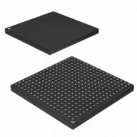
AT91SAM9M10-CU Atmel, AT91SAM9M10-CU Datasheet - Page 567

AT91SAM9M10-CU
Manufacturer Part Number
AT91SAM9M10-CU
Description
IC MCU 16/32BIT ARM9 324TFBGA
Manufacturer
Atmel
Series
AT91SAMr
Specifications of AT91SAM9M10-CU
Core Processor
ARM9
Core Size
16/32-Bit
Speed
400MHz
Connectivity
EBI/EMI, Ethernet, I²C, SPI, SSC, UART/USART, USB
Peripherals
AC'97, DMA, LCD, POR, PWM, WDT
Number Of I /o
160
Program Memory Size
64KB (64K x 8)
Program Memory Type
ROM
Ram Size
128K x 8
Voltage - Supply (vcc/vdd)
0.9 V ~ 1.1 V
Data Converters
A/D 8x10b
Oscillator Type
Internal
Operating Temperature
-40°C ~ 85°C
Package / Case
324-TFBGA
Processor Series
AT91SAMx
Core
ARM926EJ-S
Data Bus Width
32 bit
Data Ram Size
32 KB
Interface Type
2-Wire, SPI, USART
Maximum Clock Frequency
133 MHz
Number Of Programmable I/os
5
Number Of Timers
2 x 16 bit
Operating Supply Voltage
1.65 V to 3.6 V
Maximum Operating Temperature
+ 85 C
Mounting Style
SMD/SMT
3rd Party Development Tools
JTRACE-ARM-2M, MDK-ARM, RL-ARM, ULINK2
Development Tools By Supplier
AT91SAM-ICE, AT91-ISP, AT91SAM9M10-G45-EK
Controller Family/series
AT91
No. Of I/o's
160
Ram Memory Size
64KB
Cpu Speed
400MHz
No. Of Timers
2
Rohs Compliant
Yes
Cpu Family
AT91
Device Core
ARM926EJ-S
Device Core Size
32b
Frequency (max)
400MHz
Total Internal Ram Size
64KB
# I/os (max)
160
Number Of Timers - General Purpose
7
Operating Supply Voltage (typ)
1.8/2.5/3.3V
Operating Supply Voltage (max)
1.1/1.95/3.6V
Operating Supply Voltage (min)
0.9/1.65/1.8/3V
On-chip Adc
8-chx10-bit
Instruction Set Architecture
RISC
Operating Temp Range
-40C to 85C
Operating Temperature Classification
Industrial
Mounting
Surface Mount
Pin Count
324
Package Type
TFBGA
Lead Free Status / RoHS Status
Lead free / RoHS Compliant
Eeprom Size
-
Lead Free Status / Rohs Status
Lead free / RoHS Compliant
Available stocks
Company
Part Number
Manufacturer
Quantity
Price
Company:
Part Number:
AT91SAM9M10-CU
Manufacturer:
Atmel
Quantity:
996
- Current page: 567 of 1404
- Download datasheet (22Mb)
32.7.8.7
Figure 32-42. Synch Field
Figure 32-43. Slave Node Synchronization
6355B–ATARM–21-Jun-10
Fractional Part (FP)
Clcok Divider (CD)
Synchro Counter
US_BRGR
US_BRGR
Baud Rate
LINIDRX
Clock
RXD
Slave Node Synchronization
The synchronization is done only in Slave node configuration. The procedure is based on time
measurement between falling edges of the Synch Field. The falling edges are available in dis-
tances of 2, 4, 6 and 8 bit times.
The time measurement is made by a 19-bit counter clocked by the sampling clock (see
32.7.1).
When the start bit of the Synch Field is detected the counter is reset. Then during the next 8
Tbits of the Synch Field, the counter is incremented. At the end of these 8 Tbits, the counter is
stopped. At this moment, the 16 most significant bits of the counter (value divided by 8) gives the
new clock divider (CD) and the 3 least significant bits of this value (the remainder) gives the new
fractional part (FP).
When the Synch Field has been received, the clock divider (CD) and the fractional part (FP) are
updated in the Baud Rate Generator register (US_BRGR).
The accuracy of the synchronization depends on several parameters:
The following formula is used to compute the deviation of the slave bit rate relative to the master
bit rate after synchronization (F
• The nominal clock frequency (F
• The Baudrate
• The oversampling (Over=0 => 16X or Over=0 => 8X)
13 dominant bits (at 0)
Start
bit
Break Field
2 Tbit
Initial CD
Initial FP
2 Tbit
1 recessive bit
Delimiter
Break
(at 1)
8 Tbit
Synch Field
Reset
SLAVE
2 Tbit
Start
Bit
Nom
1
is the real slave node clock frequency).
) (the theoretical slave node clock frequency)
0
Synch Byte = 0x55
1
2 Tbit
0
1
0
1
0
000_0011_0001_0110_1101
Stop
Bit
Stop
0000_0110_0010_1101
101
bit
Start
Bit
ID0 ID1 ID2 ID3 ID4 ID5 ID6 ID7
AT91SAM9M10
Stop
Bit
Section
567
Related parts for AT91SAM9M10-CU
Image
Part Number
Description
Manufacturer
Datasheet
Request
R

Part Number:
Description:
MCU, MPU & DSP Development Tools KICKSTART KIT FOR AT91SAM9 PLUS
Manufacturer:
IAR Systems

Part Number:
Description:
DEV KIT FOR AVR/AVR32
Manufacturer:
Atmel
Datasheet:

Part Number:
Description:
INTERVAL AND WIPE/WASH WIPER CONTROL IC WITH DELAY
Manufacturer:
ATMEL Corporation
Datasheet:

Part Number:
Description:
Low-Voltage Voice-Switched IC for Hands-Free Operation
Manufacturer:
ATMEL Corporation
Datasheet:

Part Number:
Description:
MONOLITHIC INTEGRATED FEATUREPHONE CIRCUIT
Manufacturer:
ATMEL Corporation
Datasheet:

Part Number:
Description:
AM-FM Receiver IC U4255BM-M
Manufacturer:
ATMEL Corporation
Datasheet:

Part Number:
Description:
Monolithic Integrated Feature Phone Circuit
Manufacturer:
ATMEL Corporation
Datasheet:

Part Number:
Description:
Multistandard Video-IF and Quasi Parallel Sound Processing
Manufacturer:
ATMEL Corporation
Datasheet:

Part Number:
Description:
High-performance EE PLD
Manufacturer:
ATMEL Corporation
Datasheet:

Part Number:
Description:
8-bit Flash Microcontroller
Manufacturer:
ATMEL Corporation
Datasheet:

Part Number:
Description:
2-Wire Serial EEPROM
Manufacturer:
ATMEL Corporation
Datasheet:


