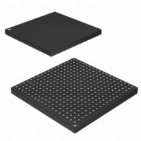
AT91SAM9M10-CU Atmel, AT91SAM9M10-CU Datasheet - Page 1372

AT91SAM9M10-CU
Manufacturer Part Number
AT91SAM9M10-CU
Description
IC MCU 16/32BIT ARM9 324TFBGA
Manufacturer
Atmel
Series
AT91SAMr
Specifications of AT91SAM9M10-CU
Core Processor
ARM9
Core Size
16/32-Bit
Speed
400MHz
Connectivity
EBI/EMI, Ethernet, I²C, SPI, SSC, UART/USART, USB
Peripherals
AC'97, DMA, LCD, POR, PWM, WDT
Number Of I /o
160
Program Memory Size
64KB (64K x 8)
Program Memory Type
ROM
Ram Size
128K x 8
Voltage - Supply (vcc/vdd)
0.9 V ~ 1.1 V
Data Converters
A/D 8x10b
Oscillator Type
Internal
Operating Temperature
-40°C ~ 85°C
Package / Case
324-TFBGA
Processor Series
AT91SAMx
Core
ARM926EJ-S
Data Bus Width
32 bit
Data Ram Size
32 KB
Interface Type
2-Wire, SPI, USART
Maximum Clock Frequency
133 MHz
Number Of Programmable I/os
5
Number Of Timers
2 x 16 bit
Operating Supply Voltage
1.65 V to 3.6 V
Maximum Operating Temperature
+ 85 C
Mounting Style
SMD/SMT
3rd Party Development Tools
JTRACE-ARM-2M, MDK-ARM, RL-ARM, ULINK2
Development Tools By Supplier
AT91SAM-ICE, AT91-ISP, AT91SAM9M10-G45-EK
Controller Family/series
AT91
No. Of I/o's
160
Ram Memory Size
64KB
Cpu Speed
400MHz
No. Of Timers
2
Rohs Compliant
Yes
Cpu Family
AT91
Device Core
ARM926EJ-S
Device Core Size
32b
Frequency (max)
400MHz
Total Internal Ram Size
64KB
# I/os (max)
160
Number Of Timers - General Purpose
7
Operating Supply Voltage (typ)
1.8/2.5/3.3V
Operating Supply Voltage (max)
1.1/1.95/3.6V
Operating Supply Voltage (min)
0.9/1.65/1.8/3V
On-chip Adc
8-chx10-bit
Instruction Set Architecture
RISC
Operating Temp Range
-40C to 85C
Operating Temperature Classification
Industrial
Mounting
Surface Mount
Pin Count
324
Package Type
TFBGA
Lead Free Status / RoHS Status
Lead free / RoHS Compliant
Eeprom Size
-
Lead Free Status / Rohs Status
Lead free / RoHS Compliant
Available stocks
Company
Part Number
Manufacturer
Quantity
Price
Company:
Part Number:
AT91SAM9M10-CU
Manufacturer:
Atmel
Quantity:
996
- Current page: 1372 of 1404
- Download datasheet (22Mb)
Table 47-36. SSC Timings with 3.3V Peripheral Supply
Notes:
Table 47-37. SSC Timings with 1.8V Peripheral Supply
Notes:
1372
Symbol
SSC
SSC
SSC
Symbol
SSC
SSC
SSC
SSC
SSC
SSC
SSC
SSC
SSC
SSC
SSC
SSC
SSC
SSC
11
12
13
0
1
2
3
4
5
6
7
8
9
10
11
12
13
(1)
(1)
1. Timings SSC4 and SSC7 depend on the start condition. When STTDLY = 0 (Receive start delay) and START = 4, or 5 or 7
2. For output signals (TF, TD, RF), Min and Max access times are defined. The Min access time is the time between the TK (or
1. Timings SSC4 and SSC7 depend on the start condition. When STTDLY = 0 (Receive start delay) and START = 4, or 5 or 7
2. For output signals (TF, TD, RF), Min and Max access times are defined. The Min access time is the time between the TK (or
AT91SAM9M10
(Receive Start Selection), two Periods of the MCK must be added to timings.
RK) edge and the signal change. The Max access time is the time between the TK edge and the signal stabilization.
47-18
(Receive Start Selection), two Periods of the MCK must be added to timings.
RK) edge and the signal change. The Max access time is the time between the TK edge and the signal stabilization.
47-18
Parameter
TK edge to TF/TD (TK output, TF output)
TK edge to TF/TD (TK input, TF output)
TF setup time before TK edge (TK output)
TF hold time after TK edge (TK output)
TK edge to TF/TD (TK output, TF input)
TF setup time before TK edge (TK input)
TF hold time after TK edge (TK input)
TK edge to TF/TD (TK input, TF input)
RF/RD setup time before RK edge (RK input)
RF/RD hold time after RK edge (RK input)
RK edge to RF (RK input)
RF/RD setup time before RK edge (RK output)
RF/RD hold time after RK edge (RK output)
RK edge to RF (RK output)
Parameter
RF/RD setup time before RK edge (RK output)
RF/RD hold time after RK edge (RK output)
RK edge to RF (RK output)
illustrates Min and Max accesses for SSC0. The same applies to SSC1, SSC4, and SSC7, SSC10 and SSC13.
illustrates Min and Max accesses for SSC0. The same applies to SSC1, SSC4, and SSC7, SSC10 and SSC13.
Transmitter
Receiver
Cond
Cond
-2.8 (+2*t
5.0 (+3*t
18.4 - t
18.6 - t
14.2 - t
t
t
t
CPMCK
CPMCK
CPMCK
t
t
4.8
5.4
CPMCK
CPMCK
Min
0
Min
0
0
0.6
2.4
CPMCK
CPMCK
(2)
(2)
(2)
CPMCK
CPMCK
CPMCK
(2)
(2)
- 5.1
- 5.1
- 3.9
)
)
(1)(2)
(1)(2)
18.3 (+3*t
4.2 (+2*t
18.4
21.5
4.2
5.3
5.2
Max
Max
CPMCK
CPMCK
(2)
(2)
(2)
(2)
(2)
)
)
(1)(2)
6355B–ATARM–21-Jun-10
(1)(2)
Units
Unit
ns
ns
ns
ns
ns
ns
ns
ns
ns
ns
ns
ns
ns
ns
ns
ns
ns
s
Figure
Figure
Related parts for AT91SAM9M10-CU
Image
Part Number
Description
Manufacturer
Datasheet
Request
R

Part Number:
Description:
MCU, MPU & DSP Development Tools KICKSTART KIT FOR AT91SAM9 PLUS
Manufacturer:
IAR Systems

Part Number:
Description:
DEV KIT FOR AVR/AVR32
Manufacturer:
Atmel
Datasheet:

Part Number:
Description:
INTERVAL AND WIPE/WASH WIPER CONTROL IC WITH DELAY
Manufacturer:
ATMEL Corporation
Datasheet:

Part Number:
Description:
Low-Voltage Voice-Switched IC for Hands-Free Operation
Manufacturer:
ATMEL Corporation
Datasheet:

Part Number:
Description:
MONOLITHIC INTEGRATED FEATUREPHONE CIRCUIT
Manufacturer:
ATMEL Corporation
Datasheet:

Part Number:
Description:
AM-FM Receiver IC U4255BM-M
Manufacturer:
ATMEL Corporation
Datasheet:

Part Number:
Description:
Monolithic Integrated Feature Phone Circuit
Manufacturer:
ATMEL Corporation
Datasheet:

Part Number:
Description:
Multistandard Video-IF and Quasi Parallel Sound Processing
Manufacturer:
ATMEL Corporation
Datasheet:

Part Number:
Description:
High-performance EE PLD
Manufacturer:
ATMEL Corporation
Datasheet:

Part Number:
Description:
8-bit Flash Microcontroller
Manufacturer:
ATMEL Corporation
Datasheet:

Part Number:
Description:
2-Wire Serial EEPROM
Manufacturer:
ATMEL Corporation
Datasheet:


