DF2239TF16I Renesas Electronics America, DF2239TF16I Datasheet - Page 168
DF2239TF16I
Manufacturer Part Number
DF2239TF16I
Description
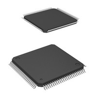
MCU 3V 384K I-TEMP 100-TQFP
Manufacturer
Renesas Electronics America
Series
H8® H8S/2200r
Datasheet
1.DF2238RFA6V.pdf
(1048 pages)
Specifications of DF2239TF16I
Core Processor
H8S/2000
Core Size
16-Bit
Speed
16MHz
Connectivity
I²C, SCI, SmartCard
Peripherals
DMA, POR, PWM, WDT
Number Of I /o
72
Program Memory Size
384KB (384K x 8)
Program Memory Type
FLASH
Ram Size
32K x 8
Voltage - Supply (vcc/vdd)
2.7 V ~ 3.6 V
Data Converters
A/D 8x10b; D/A 2x8b
Oscillator Type
Internal
Operating Temperature
-40°C ~ 85°C
Package / Case
100-TQFP, 100-VQFP
Lead Free Status / RoHS Status
Contains lead / RoHS non-compliant
Eeprom Size
-
Other names
HD64F2239TF16I
HD64F2239TF16I
HD64F2239TF16I


Section 3 MCU Operating Modes
3.3
3.3.1
The CPU can access a 16-Mbyte address space in advanced mode. The on-chip ROM is disabled.
Pins P13 to P10, and ports A, B, and C function as an address bus, ports D and E function as a
data bus, and part of port F carries bus control signals.
Pins P13 to P11 function as input ports immediately after a reset. Pin 10 and ports A and B
function as address (A20 to A8) outputs immediately after a reset. Address (A23 to A21) output
can be enabled or disabled by bits AE3 to AE0 in the pin function control register (PFCR)
regardless of the corresponding data direction register (DDR) values. Pins for which address
output is disabled among pins P13 to P10 and in ports A and B become port outputs when the
corresponding DDR bits are set to 1.
Port C always has an address (A7 to A0) output function.
The initial bus mode after a reset is 16 bits, with 16-bit access to all areas. However, note that if 8-
bit access is designated by the bus controller for all areas, the bus mode switches to 8 bits.
3.3.2
The CPU can access a 16-Mbyte address space in advanced mode. The on-chip ROM is disabled.
Pins P13 to P10, and ports A, B, and C function as an address bus, ports D and E function as a
data bus, and part of port F carries bus control signals.
Pins P13 to P11 function as input ports immediately after a reset. Pin 10 and ports A and B
function as address (A20 to A8) outputs immediately after a reset. Address (A23 to A21) output
can be enabled or disabled by bits AE3 to AE0 in the pin function control register (PFCR)
regardless of the corresponding data direction register (DDR) values. Pins for which address
output is disabled among pins P13 to P10 and in ports A and B become port outputs when the
corresponding DDR bits are set to 1.
Port C always has an address (A7 to A0) output function.
The initial bus mode after a reset is 8 bits, with 8-bit access to all areas. However, note that if 16-
bit access is designated by the bus controller for any area, the bus mode switches to 16 bits and
port E becomes a data bus.
Rev. 6.00 Mar. 18, 2010 Page 106 of 982
REJ09B0054-0600
Mode 4
Mode 5
Operating Mode Descriptions
Related parts for DF2239TF16I
Image
Part Number
Description
Manufacturer
Datasheet
Request
R

Part Number:
Description:
CONN SOCKET 2POS 7.92MM WHITE
Manufacturer:
Hirose Electric Co Ltd
Datasheet:

Part Number:
Description:
CONN SOCKET 4POS 7.92MM WHITE
Manufacturer:
Hirose Electric Co Ltd
Datasheet:

Part Number:
Description:
CONN SOCKET 5POS 7.92MM WHITE
Manufacturer:
Hirose Electric Co Ltd
Datasheet:

Part Number:
Description:
CONN SOCKET 3POS 7.92MM WHITE
Manufacturer:
Hirose Electric Co Ltd
Datasheet:
Part Number:
Description:
CONN SOCKET 5POS 7.92MM WHITE
Manufacturer:
Hirose Electric Co Ltd
Datasheet:

Part Number:
Description:
CONN SOCKET 2POS 7.92MM WHITE
Manufacturer:
Hirose Electric Co Ltd
Datasheet:
Part Number:
Description:
CONN SOCKET 3POS 7.92MM WHITE
Manufacturer:
Hirose Electric Co Ltd
Datasheet:
Part Number:
Description:
CONN SOCKET 4POS 7.92MM WHITE
Manufacturer:
Hirose Electric Co Ltd
Datasheet:

Part Number:
Description:
CONN HEADER 2POS 7.92MM R/A TIN
Manufacturer:
Hirose Electric Co Ltd
Datasheet:

Part Number:
Description:
CONN HEADER 4POS 7.92MM R/A TIN
Manufacturer:
Hirose Electric Co Ltd
Datasheet:

Part Number:
Description:
KIT STARTER FOR M16C/29
Manufacturer:
Renesas Electronics America
Datasheet:

Part Number:
Description:
KIT STARTER FOR R8C/2D
Manufacturer:
Renesas Electronics America
Datasheet:

Part Number:
Description:
R0K33062P STARTER KIT
Manufacturer:
Renesas Electronics America
Datasheet:

Part Number:
Description:
KIT STARTER FOR R8C/23 E8A
Manufacturer:
Renesas Electronics America
Datasheet:

Part Number:
Description:
KIT STARTER FOR R8C/25
Manufacturer:
Renesas Electronics America
Datasheet: