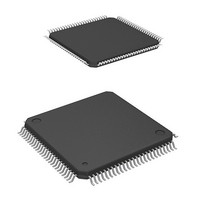
DF2239TF16I Renesas Electronics America, DF2239TF16I Datasheet - Page 742

DF2239TF16I
Manufacturer Part Number
DF2239TF16I
Description
MCU 3V 384K I-TEMP 100-TQFP
Manufacturer
Renesas Electronics America
Series
H8® H8S/2200r
Datasheet
1.DF2238RFA6V.pdf
(1048 pages)
Specifications of DF2239TF16I
Core Processor
H8S/2000
Core Size
16-Bit
Speed
16MHz
Connectivity
I²C, SCI, SmartCard
Peripherals
DMA, POR, PWM, WDT
Number Of I /o
72
Program Memory Size
384KB (384K x 8)
Program Memory Type
FLASH
Ram Size
32K x 8
Voltage - Supply (vcc/vdd)
2.7 V ~ 3.6 V
Data Converters
A/D 8x10b; D/A 2x8b
Oscillator Type
Internal
Operating Temperature
-40°C ~ 85°C
Package / Case
100-TQFP, 100-VQFP
Lead Free Status / RoHS Status
Contains lead / RoHS non-compliant
Eeprom Size
-
Other names
HD64F2239TF16I
HD64F2239TF16I
HD64F2239TF16I
- Current page: 742 of 1048
- Download datasheet (6Mb)
Section 16 I
7. Note on ICDR Read at End of Master Reception
Rev. 6.00 Mar. 18, 2010 Page 680 of 982
REJ09B0054-0600
SCL
Internal clock
SDA
BBSY bit
To halt reception after completion of a receive operation in master receive mode, set the TRS
bit to 1 and write 0 to BBSY and SCP in ICCR. This changes the SDA pin from low to high
when the SCL pin is high, and generates the stop condition. After this, receive data can be read
by means of an ICDR read, but if data remains in the buffer the ICDRS receive data will not be
transferred to ICDR, and so it will not be possible to read the second byte of data. If it is
necessary to read the second byte of data, issue the stop condition in master receive mode (i.e.
with the TRS bit cleared to 0). When reading the receive data, first confirm that the BBSY bit
in ICCR is cleared to 0, the stop condition has been generated, and the bus has been released,
then read ICDR with TRS cleared to 0. Note that if the receive data (ICDR data) is read in the
interval between execution of the instruction for issuance of the stop condition (writing of 0 to
BBSY and SCP in ICCR) and the actual generation of the stop condition, the clock may not be
output correctly in subsequent master transmission.
Clearing of the MST bit after completion of master transmission/reception, or other
modifications of IIC control bits to change the transmit/receive operating mode or settings,
must be carried out during interval (a) in figure 16.21 (after confirming that the BBSY bit has
been cleared to 0 in the ICCR register).
Figure 16.21 Points for Attention Concerning Reading of Master Receive Data
6. Value when the IICX bit is set to 1. When the IICX bit is cleared to 0, the value is 6t
7. The H8S/2258 Group is out of operation.
2
C Bus Interface (IIC) (Option)
Master receive mode
Bit 0
8
A
9
Execution of stop
condition issuance
instruction
(0 written to BBSY
and SCP)
ICDR reading
prohibited
Confirmation of stop
condition generation
(0 read from BBSY)
Stop condition
(a)
Start condition
issuance
Start condition
cyc
.
Related parts for DF2239TF16I
Image
Part Number
Description
Manufacturer
Datasheet
Request
R

Part Number:
Description:
CONN SOCKET 2POS 7.92MM WHITE
Manufacturer:
Hirose Electric Co Ltd
Datasheet:

Part Number:
Description:
CONN SOCKET 4POS 7.92MM WHITE
Manufacturer:
Hirose Electric Co Ltd
Datasheet:

Part Number:
Description:
CONN SOCKET 5POS 7.92MM WHITE
Manufacturer:
Hirose Electric Co Ltd
Datasheet:

Part Number:
Description:
CONN SOCKET 3POS 7.92MM WHITE
Manufacturer:
Hirose Electric Co Ltd
Datasheet:

Part Number:
Description:
CONN SOCKET 5POS 7.92MM WHITE
Manufacturer:
Hirose Electric Co Ltd
Datasheet:

Part Number:
Description:
CONN SOCKET 2POS 7.92MM WHITE
Manufacturer:
Hirose Electric Co Ltd
Datasheet:

Part Number:
Description:
CONN SOCKET 3POS 7.92MM WHITE
Manufacturer:
Hirose Electric Co Ltd
Datasheet:

Part Number:
Description:
CONN SOCKET 4POS 7.92MM WHITE
Manufacturer:
Hirose Electric Co Ltd
Datasheet:

Part Number:
Description:
CONN HEADER 2POS 7.92MM R/A TIN
Manufacturer:
Hirose Electric Co Ltd
Datasheet:

Part Number:
Description:
CONN HEADER 4POS 7.92MM R/A TIN
Manufacturer:
Hirose Electric Co Ltd
Datasheet:

Part Number:
Description:
KIT STARTER FOR M16C/29
Manufacturer:
Renesas Electronics America
Datasheet:

Part Number:
Description:
KIT STARTER FOR R8C/2D
Manufacturer:
Renesas Electronics America
Datasheet:

Part Number:
Description:
R0K33062P STARTER KIT
Manufacturer:
Renesas Electronics America
Datasheet:

Part Number:
Description:
KIT STARTER FOR R8C/23 E8A
Manufacturer:
Renesas Electronics America
Datasheet:

Part Number:
Description:
KIT STARTER FOR R8C/25
Manufacturer:
Renesas Electronics America
Datasheet:


