DF2239TF16I Renesas Electronics America, DF2239TF16I Datasheet - Page 674
DF2239TF16I
Manufacturer Part Number
DF2239TF16I
Description
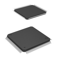
MCU 3V 384K I-TEMP 100-TQFP
Manufacturer
Renesas Electronics America
Series
H8® H8S/2200r
Datasheet
1.DF2238RFA6V.pdf
(1048 pages)
Specifications of DF2239TF16I
Core Processor
H8S/2000
Core Size
16-Bit
Speed
16MHz
Connectivity
I²C, SCI, SmartCard
Peripherals
DMA, POR, PWM, WDT
Number Of I /o
72
Program Memory Size
384KB (384K x 8)
Program Memory Type
FLASH
Ram Size
32K x 8
Voltage - Supply (vcc/vdd)
2.7 V ~ 3.6 V
Data Converters
A/D 8x10b; D/A 2x8b
Oscillator Type
Internal
Operating Temperature
-40°C ~ 85°C
Package / Case
100-TQFP, 100-VQFP
Lead Free Status / RoHS Status
Contains lead / RoHS non-compliant
Eeprom Size
-
Other names
HD64F2239TF16I
HD64F2239TF16I
HD64F2239TF16I


Section 15 Serial Communication Interface (SCI)
state Z. In this LSI, the SINV bit inverts only data bits D0 to D7. Therefore, set the O/E bit in
SMR to 1 to invert the parity bit for both transmission and reception.
15.7.3
Operation in block transfer mode is the same as that in the normal Smart Card interface mode,
except for the following points.
• In reception, though the parity check is performed, no error signal is output even if an error is
• In transmission, a guard time of at least 1 etu is left between the end of the parity bit and the
• In transmission, because retransmission is not performed, the TEND flag is set to 1, 11.5 etu
• As with the normal Smart Card interface, the ERS flag indicates the error signal status, but
15.7.4
In Smart Card interface mode an internal clock generated by the on-chip baud rate generator can
only be used as a transmission/reception clock. In this mode, the SCI operates on a base clock with
a frequency of 32, 64, 372, or 256 times the transfer rate (fixed to 16 times in normal
asynchronous mode) as determined by bits BCP1 and BCP0. In reception, the SCI samples the
falling edge of the start bit using the base clock, and performs internal synchronization. As shown
in figure 15.28, by sampling receive data at the rising-edge of the 16th, 32nd, 186th, or 128th
pulse of the base clock, data can be latched at the middle of the bit. The reception margin is given
by the following formula.
M = | (0.5 −
Where M: Reception margin (%)
Assuming values of F = 0, D = 0.5 and N = 372 in the above formula, the reception margin
formula is as follows.
Rev. 6.00 Mar. 18, 2010 Page 612 of 982
REJ09B0054-0600
detected. However, the PER bit in SSR is set to 1 and must be cleared before receiving the
parity bit of the next frame.
start of the next frame.
after transmission start.
since error signal transfer is not performed, this flag is always cleared to 0.
Receive Data Sampling Timing and Reception Margin
N: Ratio of bit rate to clock (N = 32, 64, 372, and 256)
D: Clock duty (D = 0 to 1.0)
L: Frame length (L = 10)
F: Absolute value of clock frequency deviation
Block Transfer Mode
2N
1
) − (L − 0.5) F −
| D − 0.5 |
N
(1 + F) | × 100%
Related parts for DF2239TF16I
Image
Part Number
Description
Manufacturer
Datasheet
Request
R

Part Number:
Description:
CONN SOCKET 2POS 7.92MM WHITE
Manufacturer:
Hirose Electric Co Ltd
Datasheet:

Part Number:
Description:
CONN SOCKET 4POS 7.92MM WHITE
Manufacturer:
Hirose Electric Co Ltd
Datasheet:

Part Number:
Description:
CONN SOCKET 5POS 7.92MM WHITE
Manufacturer:
Hirose Electric Co Ltd
Datasheet:

Part Number:
Description:
CONN SOCKET 3POS 7.92MM WHITE
Manufacturer:
Hirose Electric Co Ltd
Datasheet:
Part Number:
Description:
CONN SOCKET 5POS 7.92MM WHITE
Manufacturer:
Hirose Electric Co Ltd
Datasheet:

Part Number:
Description:
CONN SOCKET 2POS 7.92MM WHITE
Manufacturer:
Hirose Electric Co Ltd
Datasheet:
Part Number:
Description:
CONN SOCKET 3POS 7.92MM WHITE
Manufacturer:
Hirose Electric Co Ltd
Datasheet:
Part Number:
Description:
CONN SOCKET 4POS 7.92MM WHITE
Manufacturer:
Hirose Electric Co Ltd
Datasheet:

Part Number:
Description:
CONN HEADER 2POS 7.92MM R/A TIN
Manufacturer:
Hirose Electric Co Ltd
Datasheet:

Part Number:
Description:
CONN HEADER 4POS 7.92MM R/A TIN
Manufacturer:
Hirose Electric Co Ltd
Datasheet:

Part Number:
Description:
KIT STARTER FOR M16C/29
Manufacturer:
Renesas Electronics America
Datasheet:

Part Number:
Description:
KIT STARTER FOR R8C/2D
Manufacturer:
Renesas Electronics America
Datasheet:

Part Number:
Description:
R0K33062P STARTER KIT
Manufacturer:
Renesas Electronics America
Datasheet:

Part Number:
Description:
KIT STARTER FOR R8C/23 E8A
Manufacturer:
Renesas Electronics America
Datasheet:

Part Number:
Description:
KIT STARTER FOR R8C/25
Manufacturer:
Renesas Electronics America
Datasheet: