ATEVK1105 Atmel, ATEVK1105 Datasheet - Page 201
ATEVK1105
Manufacturer Part Number
ATEVK1105
Description
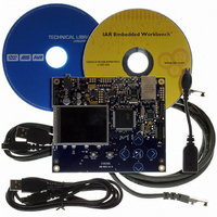
KIT EVAL FOR AT32UC3A0
Manufacturer
Atmel
Series
AVR®32r
Type
MCUr
Datasheets
1.ATAVRONE-PROBECBL.pdf
(16 pages)
2.ATEVK1104.pdf
(826 pages)
3.ATEVK1105.pdf
(28 pages)
Specifications of ATEVK1105
Contents
Evaluation Board, Software and Documentation
Processor To Be Evaluated
AT32UC3A0512
Processor Series
AVR
Data Bus Width
32 bit
Interface Type
USART, TWI, USB, SPI, Ethernet
Operating Supply Voltage
3.3 V
Silicon Manufacturer
Atmel
Core Architecture
AVR
Core Sub-architecture
AVR UC3
Silicon Core Number
AT32UC3A0512
Silicon Family Name
AVR
Kit Contents
Board CD Docs
Rohs Compliant
Yes
For Use With/related Products
AT32UC3A0
Lead Free Status / RoHS Status
Lead free / RoHS Compliant


23.7.3.3
23.7.3.4
Figure 23-7. Programmable Delays
32058J-AVR32-04/11
Chip Select 1
Chip Select 2
Clock Generation
Transfer Delays
SPCK
The SPI Baud rate clock is generated by dividing the Master Clock (MCK) or the Master Clock
divided by 32, by a value between 1 and 255. The selection between Master Clock or Master
Clock divided by 32 is done by the FDIV value set in the Mode Register
This allows a maximum operating baud rate at up to Master Clock and a minimum operating
baud rate of MCK divided by 255*32.
Programming the SCBR field at 0 is forbidden. Triggering a transfer while SCBR is at 0 can lead
to unpredictable results.
At reset, SCBR is 0 and the user has to program it at a valid value before performing the first
transfer.
The divisor can be defined independently for each chip select, as it has to be programmed in the
SCBR field of the Chip Select Registers. This allows the SPI to automatically adapt the baud
rate for each interfaced peripheral without reprogramming.
Figure 23-7
select. Three delays can be programmed to modify the transfer waveforms:
• The delay between chip selects, programmable only once for all the chip selects by writing the
• The delay before SPCK, independently programmable for each chip select by writing the field
• The delay between consecutive transfers, independently programmable for each chip select by
These delays allow the SPI to be adapted to the interfaced peripherals and their speed and bus
release time.
DLYBCS field in the Mode Register. Allows insertion of a delay between release of one chip
select and before assertion of a new one.
DLYBS. Allows the start of SPCK to be delayed after the chip select has been asserted.
writing the DLYBCT field. Allows insertion of a delay between two transfers occurring on the
same chip select
DLYBCS
shows a chip select transfer change and consecutive transfers on the same chip
DLYBS
DLYBCT
AT32UC3A
DLYBCT
201
Related parts for ATEVK1105
Image
Part Number
Description
Manufacturer
Datasheet
Request
R

Part Number:
Description:
DEV KIT FOR AVR/AVR32
Manufacturer:
Atmel
Datasheet:

Part Number:
Description:
INTERVAL AND WIPE/WASH WIPER CONTROL IC WITH DELAY
Manufacturer:
ATMEL Corporation
Datasheet:
Part Number:
Description:
Low-Voltage Voice-Switched IC for Hands-Free Operation
Manufacturer:
ATMEL Corporation
Datasheet:
Part Number:
Description:
MONOLITHIC INTEGRATED FEATUREPHONE CIRCUIT
Manufacturer:
ATMEL Corporation
Datasheet:
Part Number:
Description:
AM-FM Receiver IC U4255BM-M
Manufacturer:
ATMEL Corporation
Datasheet:
Part Number:
Description:
Monolithic Integrated Feature Phone Circuit
Manufacturer:
ATMEL Corporation
Datasheet:
Part Number:
Description:
Multistandard Video-IF and Quasi Parallel Sound Processing
Manufacturer:
ATMEL Corporation
Datasheet:
Part Number:
Description:
High-performance EE PLD
Manufacturer:
ATMEL Corporation
Datasheet:
Part Number:
Description:
8-bit Flash Microcontroller
Manufacturer:
ATMEL Corporation
Datasheet:
Part Number:
Description:
2-Wire Serial EEPROM
Manufacturer:
ATMEL Corporation
Datasheet: