ATEVK1105 Atmel, ATEVK1105 Datasheet - Page 755
ATEVK1105
Manufacturer Part Number
ATEVK1105
Description
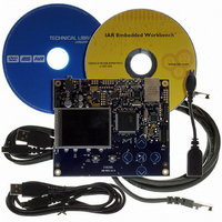
KIT EVAL FOR AT32UC3A0
Manufacturer
Atmel
Series
AVR®32r
Type
MCUr
Datasheets
1.ATAVRONE-PROBECBL.pdf
(16 pages)
2.ATEVK1104.pdf
(826 pages)
3.ATEVK1105.pdf
(28 pages)
Specifications of ATEVK1105
Contents
Evaluation Board, Software and Documentation
Processor To Be Evaluated
AT32UC3A0512
Processor Series
AVR
Data Bus Width
32 bit
Interface Type
USART, TWI, USB, SPI, Ethernet
Operating Supply Voltage
3.3 V
Silicon Manufacturer
Atmel
Core Architecture
AVR
Core Sub-architecture
AVR UC3
Silicon Core Number
AT32UC3A0512
Silicon Family Name
AVR
Kit Contents
Board CD Docs
Rohs Compliant
Yes
For Use With/related Products
AT32UC3A0
Lead Free Status / RoHS Status
Lead free / RoHS Compliant


36.9.6
32058J–AVR32–04/11
MEMORY_BLOCK_ACCESS
Note: This instruction was previously known as MEMORY_ACCESS, and is provided for back-
wards compatibility.
The data register is alternately interpreted by the SAB as an address register and a data regis-
ter. The SAB starts in address mode after the MEMORY_WORD_ACCESS instruction is
selected, and toggles between address and data mode each time a data scan completes with
the busy bit cleared.
Starting in Run-Test/Idle, SAB data are accessed in the following way:
For any operation, the full 34 bits of the address must be provided. For write operations, 32 data
bits must be provided, or the result will be undefined. For read operations, shifting may be termi-
nated once the required number of bits have been acquired.
Table 36-9.
This instruction allows access to the entire SAB data area. Up to 32 bits of data are accessed at
a time, while the address is sequentially incremented from the previously used address.
In this mode, the SAB address, size, and access direction is not provided with each access.
Instead, the previous address is auto-incremented depending on the specified size and the pre-
v i o u s o p e r a t i o n r e p e a t e d . T h e a d d r e s s m u s t b e s e t u p i n a d v a n c e w i t h
MEMORY_SIZE_ACCESS or MEMORY_WORD_ACCESS. It is allowed, but not required, to
shift data after shifting the address.
This instruction is primarily intended to speed up large quantities of sequential word accesses. It
is possible to use it also for byte and halfword accesses, but the overhead in this is case much
larger as 32 bits must still be shifted for each access.
The following sequence should be used:
Instructions
IR input value
IR output value
DR Size
DR input value (Address phase)
DR input value (Data read phase)
DR input value (Data write phase)
DR output value (Address phase)
DR output value (Data read phase)
DR output value (Data write phase)
1. Select the DR Scan path.
2. Scan in the 34-bit address of the data to access, and a direction bit (1=read, 0=write).
3. Go to Update-DR and re-enter Select-DR Scan.
4. For a read operation, scan out the contents of the addressed area. For a write opera-
5. Return to Run-Test/Idle.
tion, scan in the new contents of the area.
MEMORY_WORD_ACCESS details
Details
10001 (0x11)
peb01
35 bits
aaaaaaaa aaaaaaaa aaaaaaaa aaaaaaaa aar
xxxxxxxx xxxxxxxx xxxxxxxx xxxxxxxx xxx
dddddddd dddddddd dddddddd dddddddd xxx
xxxxxxxx xxxxxxxx xxxxxxxx xxxxxxxx xeb
xeb dddddddd dddddddd dddddddd dddddddd
xxx xxxxxxxx xxxxxxxx xxxxxxxx xxxxxxeb
AT32UC3A
755
Related parts for ATEVK1105
Image
Part Number
Description
Manufacturer
Datasheet
Request
R

Part Number:
Description:
DEV KIT FOR AVR/AVR32
Manufacturer:
Atmel
Datasheet:

Part Number:
Description:
INTERVAL AND WIPE/WASH WIPER CONTROL IC WITH DELAY
Manufacturer:
ATMEL Corporation
Datasheet:
Part Number:
Description:
Low-Voltage Voice-Switched IC for Hands-Free Operation
Manufacturer:
ATMEL Corporation
Datasheet:
Part Number:
Description:
MONOLITHIC INTEGRATED FEATUREPHONE CIRCUIT
Manufacturer:
ATMEL Corporation
Datasheet:
Part Number:
Description:
AM-FM Receiver IC U4255BM-M
Manufacturer:
ATMEL Corporation
Datasheet:
Part Number:
Description:
Monolithic Integrated Feature Phone Circuit
Manufacturer:
ATMEL Corporation
Datasheet:
Part Number:
Description:
Multistandard Video-IF and Quasi Parallel Sound Processing
Manufacturer:
ATMEL Corporation
Datasheet:
Part Number:
Description:
High-performance EE PLD
Manufacturer:
ATMEL Corporation
Datasheet:
Part Number:
Description:
8-bit Flash Microcontroller
Manufacturer:
ATMEL Corporation
Datasheet:
Part Number:
Description:
2-Wire Serial EEPROM
Manufacturer:
ATMEL Corporation
Datasheet: