ATEVK1105 Atmel, ATEVK1105 Datasheet - Page 334
ATEVK1105
Manufacturer Part Number
ATEVK1105
Description
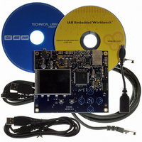
KIT EVAL FOR AT32UC3A0
Manufacturer
Atmel
Series
AVR®32r
Type
MCUr
Datasheets
1.ATAVRONE-PROBECBL.pdf
(16 pages)
2.ATEVK1104.pdf
(826 pages)
3.ATEVK1105.pdf
(28 pages)
Specifications of ATEVK1105
Contents
Evaluation Board, Software and Documentation
Processor To Be Evaluated
AT32UC3A0512
Processor Series
AVR
Data Bus Width
32 bit
Interface Type
USART, TWI, USB, SPI, Ethernet
Operating Supply Voltage
3.3 V
Silicon Manufacturer
Atmel
Core Architecture
AVR
Core Sub-architecture
AVR UC3
Silicon Core Number
AT32UC3A0512
Silicon Family Name
AVR
Kit Contents
Board CD Docs
Rohs Compliant
Yes
For Use With/related Products
AT32UC3A0
Lead Free Status / RoHS Status
Lead free / RoHS Compliant


26.7.8.2
26.7.8.3
32058J–AVR32–04/11
Data Transfer
Baud Rate
In SPI Mode, the baudrate generator operates in the same way as in USART synchronous
mode:
In SPI Master Mode:
• the external clock CLK must not be selected (USCLKS … 0x3), and the bit CLKO must be set
• to obtain correct behavior of the receiver and the transmitter, the value programmed in CD of
• if the internal clock divided (CLK_USART/DIV) is selected, the value programmed in CD must
In SPI Slave Mode:
• the external clock (CLK) selection is forced regardless of the value of the USCLKS field in the
• to obtain correct behavior of the receiver and the transmitter, the external clock (CLK)
Up to 9 data bits are successively shifted out on the TXD pin at each rising or falling edge
(depending of CPOL and CPHA) of the programmed serial clock. There is no Start bit, no Parity
bit and no Stop bit.
The number of data bits is selected by the CHRL field and the MODE 9 bit in the Mode Register
(MR). The 9 bits are selected by setting the MODE 9 bit regardless of the CHRL field. The MSB
data bit is always sent first in SPI Mode (Master or Slave).
Four combinations of polarity and phase are available for data transfers. The clock polarity is
programmed with the CPOL bit in the Mode Register. The clock phase is programmed with the
CPHA bit. These two parameters determine the edges of the clock signal upon which data is
driven and sampled. Each of the two parameters has two possible states, resulting in four possi-
ble combinations that are incompatible with one another. Thus, a master/slave pair must use the
same parameter pair values to communicate. If multiple slaves are used and fixed in different
configurations, the master must reconfigure itself each time it needs to communicate with a dif-
ferent slave.
Table 26-11. SPI Bus Protocol Mode
to “1” in the Mode Register (MR), in order to generate correctly the serial clock on the CLK pin.
must be superior or equal to 4.
be even to ensure a 50:50 mark/space ratio on the CLK pin, this value can be odd if the
internal clock is selected (CLK_USART).
Mode Register (MR). Likewise, the value written in BRGR has no effect, because the clock is
provided directly by the signal on the USART CLK pin.
frequency must be at least 4 times lower than the system clock.
See Section “26.7.1.4” on page 307.
SPI Bus Protocol Mode
0
1
2
3
However, there are some restrictions:
CPOL
0
0
1
1
AT32UC3A
CPHA
1
0
1
0
334
Related parts for ATEVK1105
Image
Part Number
Description
Manufacturer
Datasheet
Request
R

Part Number:
Description:
DEV KIT FOR AVR/AVR32
Manufacturer:
Atmel
Datasheet:

Part Number:
Description:
INTERVAL AND WIPE/WASH WIPER CONTROL IC WITH DELAY
Manufacturer:
ATMEL Corporation
Datasheet:
Part Number:
Description:
Low-Voltage Voice-Switched IC for Hands-Free Operation
Manufacturer:
ATMEL Corporation
Datasheet:
Part Number:
Description:
MONOLITHIC INTEGRATED FEATUREPHONE CIRCUIT
Manufacturer:
ATMEL Corporation
Datasheet:
Part Number:
Description:
AM-FM Receiver IC U4255BM-M
Manufacturer:
ATMEL Corporation
Datasheet:
Part Number:
Description:
Monolithic Integrated Feature Phone Circuit
Manufacturer:
ATMEL Corporation
Datasheet:
Part Number:
Description:
Multistandard Video-IF and Quasi Parallel Sound Processing
Manufacturer:
ATMEL Corporation
Datasheet:
Part Number:
Description:
High-performance EE PLD
Manufacturer:
ATMEL Corporation
Datasheet:
Part Number:
Description:
8-bit Flash Microcontroller
Manufacturer:
ATMEL Corporation
Datasheet:
Part Number:
Description:
2-Wire Serial EEPROM
Manufacturer:
ATMEL Corporation
Datasheet: