ATEVK1105 Atmel, ATEVK1105 Datasheet - Page 261
ATEVK1105
Manufacturer Part Number
ATEVK1105
Description
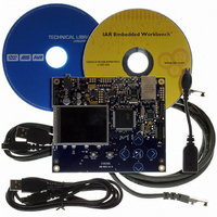
KIT EVAL FOR AT32UC3A0
Manufacturer
Atmel
Series
AVR®32r
Type
MCUr
Datasheets
1.ATAVRONE-PROBECBL.pdf
(16 pages)
2.ATEVK1104.pdf
(826 pages)
3.ATEVK1105.pdf
(28 pages)
Specifications of ATEVK1105
Contents
Evaluation Board, Software and Documentation
Processor To Be Evaluated
AT32UC3A0512
Processor Series
AVR
Data Bus Width
32 bit
Interface Type
USART, TWI, USB, SPI, Ethernet
Operating Supply Voltage
3.3 V
Silicon Manufacturer
Atmel
Core Architecture
AVR
Core Sub-architecture
AVR UC3
Silicon Core Number
AT32UC3A0512
Silicon Family Name
AVR
Kit Contents
Board CD Docs
Rohs Compliant
Yes
For Use With/related Products
AT32UC3A0
Lead Free Status / RoHS Status
Lead free / RoHS Compliant


25.5
Table 25-1.
25.6
25.6.1
25.6.2
25.6.3
25.7
32058J-AVR32-04/11
Pin Name
RX_FRAME_SYNC
RX_CLOCK
RX_DATA
TX_FRAME_SYNC
TX_CLOCK
TX_DATA
I/O Lines Description
Product Dependencies
Functional Description
I/O Lines
Power Management
Interrupt
I/O Lines Description
The pins used for interfacing the compliant external devices may be multiplexed with PIO lines.
Before using the SSC receiver, the PIO controller must be configured to dedicate the SSC
receiver I/O lines to the SSC peripheral mode.
Before using the SSC transmitter, the PIO controller must be configured to dedicate the SSC
transmitter I/O lines to the SSC peripheral mode.
The SSC clock is generated by the power manager. Before using the SSC, the programmer
must ensure that the SSC clock is enabled in the power manager.
In the SSC description, Master Clock (CLK_SSC) is the bus clock of the peripheral bus to which
the SSC is connected.
The SSC interface has an interrupt line connected to the interrupt controller. Handling interrupts
requires programming the interrupt controller before configuring the SSC.
All SSC interrupts can be enabled/disabled configuring the SSC Interrupt mask register. Each
pending and unmasked SSC interrupt will assert the SSC interrupt line. The SSC interrupt ser-
vice routine can get the interrupt origin by reading the SSC interrupt status register.
This chapter contains the functional description of the following: SSC Functional Block, Clock
Management, Data format, Start, Transmitter, Receiver and Frame Sync.
The receiver and transmitter operate separately. However, they can work synchronously by pro-
gramming the receiver to use the transmit clock and/or to start a data transfer when transmission
starts. Alternatively, this can be done by programming the transmitter to use the receive clock
and/or to start a data transfer when reception starts. The transmitter and the receiver can be pro-
grammed to operate with the clock signals provided on either the TX_CLOCK or RX_CLOCK
pins. This allows the SSC to support many slave-mode data transfers. The maximum clock
speed allowed on the TX_CLOCK and RX_CLOCK pins is the master clock divided by 2.
Pin Description
Receiver Frame Synchro
Receiver Clock
Receiver Data
Transmitter Frame Synchro
Transmitter Clock
Transmitter Data
AT32UC3A
Input/Output
Input/Output
Input/Output
Input/Output
Output
Type
Input
261
Related parts for ATEVK1105
Image
Part Number
Description
Manufacturer
Datasheet
Request
R

Part Number:
Description:
DEV KIT FOR AVR/AVR32
Manufacturer:
Atmel
Datasheet:

Part Number:
Description:
INTERVAL AND WIPE/WASH WIPER CONTROL IC WITH DELAY
Manufacturer:
ATMEL Corporation
Datasheet:
Part Number:
Description:
Low-Voltage Voice-Switched IC for Hands-Free Operation
Manufacturer:
ATMEL Corporation
Datasheet:
Part Number:
Description:
MONOLITHIC INTEGRATED FEATUREPHONE CIRCUIT
Manufacturer:
ATMEL Corporation
Datasheet:
Part Number:
Description:
AM-FM Receiver IC U4255BM-M
Manufacturer:
ATMEL Corporation
Datasheet:
Part Number:
Description:
Monolithic Integrated Feature Phone Circuit
Manufacturer:
ATMEL Corporation
Datasheet:
Part Number:
Description:
Multistandard Video-IF and Quasi Parallel Sound Processing
Manufacturer:
ATMEL Corporation
Datasheet:
Part Number:
Description:
High-performance EE PLD
Manufacturer:
ATMEL Corporation
Datasheet:
Part Number:
Description:
8-bit Flash Microcontroller
Manufacturer:
ATMEL Corporation
Datasheet:
Part Number:
Description:
2-Wire Serial EEPROM
Manufacturer:
ATMEL Corporation
Datasheet: