ATEVK1105 Atmel, ATEVK1105 Datasheet - Page 202
ATEVK1105
Manufacturer Part Number
ATEVK1105
Description
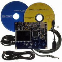
KIT EVAL FOR AT32UC3A0
Manufacturer
Atmel
Series
AVR®32r
Type
MCUr
Datasheets
1.ATAVRONE-PROBECBL.pdf
(16 pages)
2.ATEVK1104.pdf
(826 pages)
3.ATEVK1105.pdf
(28 pages)
Specifications of ATEVK1105
Contents
Evaluation Board, Software and Documentation
Processor To Be Evaluated
AT32UC3A0512
Processor Series
AVR
Data Bus Width
32 bit
Interface Type
USART, TWI, USB, SPI, Ethernet
Operating Supply Voltage
3.3 V
Silicon Manufacturer
Atmel
Core Architecture
AVR
Core Sub-architecture
AVR UC3
Silicon Core Number
AT32UC3A0512
Silicon Family Name
AVR
Kit Contents
Board CD Docs
Rohs Compliant
Yes
For Use With/related Products
AT32UC3A0
Lead Free Status / RoHS Status
Lead free / RoHS Compliant


23.7.3.5
23.7.3.6
32058J-AVR32-04/11
Peripheral Selection
Peripheral Chip Select Decoding
The serial peripherals are selected through the assertion of the NPCS0 to NPCS3 signals. By
default, all the NPCS signals are high before and after each transfer.
The peripheral selection can be performed in two different ways:
• Fixed Peripheral Select: SPI exchanges data with only one peripheral
• Variable Peripheral Select: Data can be exchanged with more than one peripheral
Fixed Peripheral Select is activated by writing the PS bit to zero in MR (Mode Register). In this
case, the current peripheral is defined by the PCS field in MR and the PCS field in TDR have no
effect.
Variable Peripheral Select is activated by setting PS bit to one. The PCS field in TDR is used to
select the current peripheral. This means that the peripheral selection can be defined for each
new data.
The Fixed Peripheral Selection allows buffer transfers with a single peripheral. Using the PDC is
an optimal means, as the size of the data transfer between the memory and the SPI is either 8
bits or 16 bits. However, changing the peripheral selection requires the Mode Register to be
reprogrammed.
The Variable Peripheral Selection allows buffer transfers with multiple peripherals without repro-
gramming the Mode Register. Data written in TDR is 32 bits wide and defines the real data to be
transmitted and the peripheral it is destined to. Using the PDC in this mode requires 32-bit wide
buffers, with the data in the LSBs and the PCS and LASTXFER fields in the MSBs, however the
SPI still controls the number of bits (8 to16) to be transferred through MISO and MOSI lines with
the chip select configuration registers. This is not the optimal means in term of memory size for
the buffers, but it provides a very effective means to exchange data with several peripherals
without any intervention of the processor.
The user can program the SPI to operate with up to 15 peripherals by decoding the four Chip
Select lines, NPCS0 to NPCS3 with an external logic. This can be enabled by writing the PCS-
DEC bit at 1 in the Mode Register (MR).
When operating without decoding, the SPI makes sure that in any case only one chip select line
is activated, i.e. driven low at a time. If two bits are defined low in a PCS field, only the lowest
numbered chip select is driven low.
When operating with decoding, the SPI directly outputs the value defined by the PCS field of
either the Mode Register or the Transmit Data Register (depending on PS).
As the SPI sets a default value of 0xF on the chip select lines (i.e. all chip select lines at 1) when
not processing any transfer, only 15 peripherals can be decoded.
The SPI has only four Chip Select Registers, not 15. As a result, when decoding is activated,
each chip select defines the characteristics of up to four peripherals. As an example, CRS0
defines the characteristics of the externally decoded peripherals 0 to 3, corresponding to the
PCS values 0x0 to 0x3. Thus, the user has to make sure to connect compatible peripherals on
the decoded chip select lines 0 to 3, 4 to 7, 8 to 11 and 12 to 14.
AT32UC3A
202
Related parts for ATEVK1105
Image
Part Number
Description
Manufacturer
Datasheet
Request
R

Part Number:
Description:
DEV KIT FOR AVR/AVR32
Manufacturer:
Atmel
Datasheet:

Part Number:
Description:
INTERVAL AND WIPE/WASH WIPER CONTROL IC WITH DELAY
Manufacturer:
ATMEL Corporation
Datasheet:
Part Number:
Description:
Low-Voltage Voice-Switched IC for Hands-Free Operation
Manufacturer:
ATMEL Corporation
Datasheet:
Part Number:
Description:
MONOLITHIC INTEGRATED FEATUREPHONE CIRCUIT
Manufacturer:
ATMEL Corporation
Datasheet:
Part Number:
Description:
AM-FM Receiver IC U4255BM-M
Manufacturer:
ATMEL Corporation
Datasheet:
Part Number:
Description:
Monolithic Integrated Feature Phone Circuit
Manufacturer:
ATMEL Corporation
Datasheet:
Part Number:
Description:
Multistandard Video-IF and Quasi Parallel Sound Processing
Manufacturer:
ATMEL Corporation
Datasheet:
Part Number:
Description:
High-performance EE PLD
Manufacturer:
ATMEL Corporation
Datasheet:
Part Number:
Description:
8-bit Flash Microcontroller
Manufacturer:
ATMEL Corporation
Datasheet:
Part Number:
Description:
2-Wire Serial EEPROM
Manufacturer:
ATMEL Corporation
Datasheet: