ATEVK1105 Atmel, ATEVK1105 Datasheet - Page 743
ATEVK1105
Manufacturer Part Number
ATEVK1105
Description
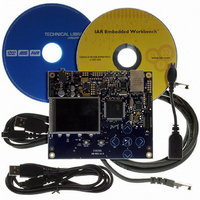
KIT EVAL FOR AT32UC3A0
Manufacturer
Atmel
Series
AVR®32r
Type
MCUr
Datasheets
1.ATAVRONE-PROBECBL.pdf
(16 pages)
2.ATEVK1104.pdf
(826 pages)
3.ATEVK1105.pdf
(28 pages)
Specifications of ATEVK1105
Contents
Evaluation Board, Software and Documentation
Processor To Be Evaluated
AT32UC3A0512
Processor Series
AVR
Data Bus Width
32 bit
Interface Type
USART, TWI, USB, SPI, Ethernet
Operating Supply Voltage
3.3 V
Silicon Manufacturer
Atmel
Core Architecture
AVR
Core Sub-architecture
AVR UC3
Silicon Core Number
AT32UC3A0512
Silicon Family Name
AVR
Kit Contents
Board CD Docs
Rohs Compliant
Yes
For Use With/related Products
AT32UC3A0
Lead Free Status / RoHS Status
Lead free / RoHS Compliant


36.4
Table 36-1.
36.5
36.5.1
36.6
36.6.1
32058J–AVR32–04/11
Name
TCK
TMS
TDI
TDO
I/O Lines Description
Product Dependencies
Functional description
I/O Lines
JTAG interface
I/O Lines Description
Description
Test Mode Select, sampled on rising TCK
Test Clock Input. Fully asynchronous to system clock frequency.
Test Data In, sampled on rising TCK.
Test Data Out, driven on falling TCK.
In order to use this module, other parts of the system must be configured correctly, as described
below.
The JTAG interface pins are multiplexed with IO lines. When the JTAG is used the associated
pins must be enabled. To enable the JTAG pins TCK must be zero while RESET_N has a zero
to one transition. To disable the JTAG pins TCK must be one while RESET_N has a zero to one
transition.
While using the JTAG lines all normal peripheral activity on these lines are disabled. The user
must make sure that no external peripheral is blocking the JTAG lines while debugging.
The JTAG interface is accessed through the dedicated JTAG pins shown in
743. The TMS control line navigates the TAP controller, as shown in
The TAP controller manages the serial access to the JTAG Instruction and Data registers. Data
is scanned into the selected instruction or data register on TDI, and out of the register on TDO,
in the Shift-IR and Shift-DR states, respectively. The LSB is shifted in and out first. TDO is high-
Z in other states than Shift-IR and Shift-DR.
Independent of the initial state of the TAP Controller, the Test-Logic-Reset state can always be
entered by holding TMS high for 5 TCK clock periods. This sequence should always be applied
at the start of a JTAG session to bring the TAP Controller into a defined state before applying
JTAG commands. Applying a 0 on TMS for 1 TCK period brings the TAP Controller to the Run-
Test/Idle state, which is the starting point for JTAG operations.
The device implements a 5-bit Instruction Register (IR). A number of public JTAG instructions
defined by the JTAG standard are supported, as described in
of AVR32-specific private JTAG instructions described in
a specific data register for the Shift-DR path, as described for each instruction.
Section
Section
36.9. Each instruction selects
Figure 36-2 on page
36.8, as well as a number
AT32UC3A
Table 36-1 on page
Type
Input
Input
Input
Output
744.
743
Related parts for ATEVK1105
Image
Part Number
Description
Manufacturer
Datasheet
Request
R

Part Number:
Description:
DEV KIT FOR AVR/AVR32
Manufacturer:
Atmel
Datasheet:

Part Number:
Description:
INTERVAL AND WIPE/WASH WIPER CONTROL IC WITH DELAY
Manufacturer:
ATMEL Corporation
Datasheet:
Part Number:
Description:
Low-Voltage Voice-Switched IC for Hands-Free Operation
Manufacturer:
ATMEL Corporation
Datasheet:
Part Number:
Description:
MONOLITHIC INTEGRATED FEATUREPHONE CIRCUIT
Manufacturer:
ATMEL Corporation
Datasheet:
Part Number:
Description:
AM-FM Receiver IC U4255BM-M
Manufacturer:
ATMEL Corporation
Datasheet:
Part Number:
Description:
Monolithic Integrated Feature Phone Circuit
Manufacturer:
ATMEL Corporation
Datasheet:
Part Number:
Description:
Multistandard Video-IF and Quasi Parallel Sound Processing
Manufacturer:
ATMEL Corporation
Datasheet:
Part Number:
Description:
High-performance EE PLD
Manufacturer:
ATMEL Corporation
Datasheet:
Part Number:
Description:
8-bit Flash Microcontroller
Manufacturer:
ATMEL Corporation
Datasheet:
Part Number:
Description:
2-Wire Serial EEPROM
Manufacturer:
ATMEL Corporation
Datasheet: