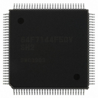
HD64F7144F50V Renesas Electronics America, HD64F7144F50V Datasheet - Page 509

HD64F7144F50V
Manufacturer Part Number
HD64F7144F50V
Description
IC SUPERH MCU FLASH 256K 112QFP
Manufacturer
Renesas Electronics America
Series
SuperH® SH7144r
Specifications of HD64F7144F50V
Core Processor
SH-2
Core Size
32-Bit
Speed
50MHz
Connectivity
EBI/EMI, I²C, SCI
Peripherals
DMA, POR, PWM, WDT
Number Of I /o
74
Program Memory Size
256KB (256K x 8)
Program Memory Type
FLASH
Ram Size
8K x 8
Voltage - Supply (vcc/vdd)
3 V ~ 3.6 V
Data Converters
A/D 8x10b
Oscillator Type
Internal
Operating Temperature
-20°C ~ 75°C
Package / Case
112-QFP
For Use With
HS0005KCU11H - EMULATOR E10A-USB H8S(X),SH2(A)EDK7145 - DEV EVALUATION KIT SH7145
Lead Free Status / RoHS Status
Lead free / RoHS Compliant
Eeprom Size
-
Available stocks
Company
Part Number
Manufacturer
Quantity
Price
Company:
Part Number:
HD64F7144F50V
Manufacturer:
RENESAS
Quantity:
450
Company:
Part Number:
HD64F7144F50V
Manufacturer:
Renesas Electronics America
Quantity:
10 000
Part Number:
HD64F7144F50V
Manufacturer:
RENESAS/瑞萨
Quantity:
20 000
- Current page: 509 of 932
- Download datasheet (6Mb)
13.9
13.9.1
The TDRE bit in the serial status register (SSR) is a status flag indicating transferring of transmit
data from TDR into TSR. The SCI sets the TDRE bit to 1 when it transfers data from TDR to
TSR.
Data can be written to TDR regardless of the TDRE bit status.
If new data is written in TDR when TDRE is 0, however, the old data stored in TDR will be lost
because the data has not yet been transferred to TSR. Before writing transmit data to TDR, be sure
to check that the TDRE bit is set to 1.
13.9.2
SCI operation can be disabled or enabled using the module standby control register. The initial
setting is for SCI operation to be halted. Register access is enabled by clearing module standby
mode. For details, refer to section 24, Power-Down Modes.
13.9.3
When framing error detection is performed, a break can be detected by reading the RxD pin value
directly. In a break, the input from the RxD pin becomes all 0s, and so the FER flag is set, and the
PER flag may also be set. Note that, since the SCI continues the receive operation after receiving a
break, even if the FER flag is cleared to 0, it will be set to 1 again.
13.9.4
The TxD pin becomes of the I/O port general I/O pin with the I/O direction and level determined
by the port data register (DR) and the port I/O register (IOR) of the pin function controller (PFC).
These conditions allow break signals to be sent.
The DR value is substituted for the marking status until the PFC is set. Consequently, the output
port is set to initially output a 1.
To send a break in serial transmission, first clear the DR to 0, then establish the TxD pin as an
output port using the PFC.
Usage Notes
TDR Write and TDRE Flag
Module Standby Mode Setting
Break Detection and Processing (Asynchronous Mode Only)
Sending Break Signal (Asynchronous Mode Only)
13. Serial Communication Interface (SCI)
Rev.4.00 Mar. 27, 2008 Page 463 of 882
REJ09B0108-0400
Related parts for HD64F7144F50V
Image
Part Number
Description
Manufacturer
Datasheet
Request
R

Part Number:
Description:
KIT STARTER FOR M16C/29
Manufacturer:
Renesas Electronics America
Datasheet:

Part Number:
Description:
KIT STARTER FOR R8C/2D
Manufacturer:
Renesas Electronics America
Datasheet:

Part Number:
Description:
R0K33062P STARTER KIT
Manufacturer:
Renesas Electronics America
Datasheet:

Part Number:
Description:
KIT STARTER FOR R8C/23 E8A
Manufacturer:
Renesas Electronics America
Datasheet:

Part Number:
Description:
KIT STARTER FOR R8C/25
Manufacturer:
Renesas Electronics America
Datasheet:

Part Number:
Description:
KIT STARTER H8S2456 SHARPE DSPLY
Manufacturer:
Renesas Electronics America
Datasheet:

Part Number:
Description:
KIT STARTER FOR R8C38C
Manufacturer:
Renesas Electronics America
Datasheet:

Part Number:
Description:
KIT STARTER FOR R8C35C
Manufacturer:
Renesas Electronics America
Datasheet:

Part Number:
Description:
KIT STARTER FOR R8CL3AC+LCD APPS
Manufacturer:
Renesas Electronics America
Datasheet:

Part Number:
Description:
KIT STARTER FOR RX610
Manufacturer:
Renesas Electronics America
Datasheet:

Part Number:
Description:
KIT STARTER FOR R32C/118
Manufacturer:
Renesas Electronics America
Datasheet:

Part Number:
Description:
KIT DEV RSK-R8C/26-29
Manufacturer:
Renesas Electronics America
Datasheet:

Part Number:
Description:
KIT STARTER FOR SH7124
Manufacturer:
Renesas Electronics America
Datasheet:

Part Number:
Description:
KIT STARTER FOR H8SX/1622
Manufacturer:
Renesas Electronics America
Datasheet:


