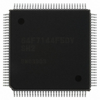
HD64F7144F50V Renesas Electronics America, HD64F7144F50V Datasheet - Page 754

HD64F7144F50V
Manufacturer Part Number
HD64F7144F50V
Description
IC SUPERH MCU FLASH 256K 112QFP
Manufacturer
Renesas Electronics America
Series
SuperH® SH7144r
Specifications of HD64F7144F50V
Core Processor
SH-2
Core Size
32-Bit
Speed
50MHz
Connectivity
EBI/EMI, I²C, SCI
Peripherals
DMA, POR, PWM, WDT
Number Of I /o
74
Program Memory Size
256KB (256K x 8)
Program Memory Type
FLASH
Ram Size
8K x 8
Voltage - Supply (vcc/vdd)
3 V ~ 3.6 V
Data Converters
A/D 8x10b
Oscillator Type
Internal
Operating Temperature
-20°C ~ 75°C
Package / Case
112-QFP
For Use With
HS0005KCU11H - EMULATOR E10A-USB H8S(X),SH2(A)EDK7145 - DEV EVALUATION KIT SH7145
Lead Free Status / RoHS Status
Lead free / RoHS Compliant
Eeprom Size
-
Available stocks
Company
Part Number
Manufacturer
Quantity
Price
Company:
Part Number:
HD64F7144F50V
Manufacturer:
RENESAS
Quantity:
450
Company:
Part Number:
HD64F7144F50V
Manufacturer:
Renesas Electronics America
Quantity:
10 000
Part Number:
HD64F7144F50V
Manufacturer:
RENESAS/瑞萨
Quantity:
20 000
- Current page: 754 of 932
- Download datasheet (6Mb)
23. Advanced User Debugger (AUD)
• Pin Functions in Branch Trace Mode
Rev.4.00 Mar. 27, 2008 Page 708 of 882
REJ09B0108-0400
Pin
AUDCK
AUDSYNC
AUDATA3 to
AUDATA0
Description
This pin outputs 1/2 the operating frequency (φ/2).
This is the clock for AUDATA synchronization.
This pin indicates whether output from AUDATA is valid.
High: Valid address data is not being output
Low: Valid address is being output
1. When AUDSYNC is low
2. When AUDSYNC is high
When a program branch or interrupt branch occurs, the AUD asserts
AUDSYNC and outputs the branch destination address. The output order is
as follows: A3 to A0, A7 to A4, A11 to A8, A15 to A12, A19 to A16, A23 to
A20, A27 to A24, A31 to A28.
When waiting for branch destination address output, these pins constantly
output 0011.
When an branch occurs, AUDATA3 and AUDATA2 output 10, and
AUDATA1 and AUDATA0 indicate whether a 4-, 8-, 16-, or 32-bit address
is to be output by comparing the previous fully output address with the
address output this time (see table below).
00
01
10
11
Address bits A31 to A4 match; 4 address bits A3 to A0 are to be
output (i.e. output is performed once).
Address bits A31 to A8 match; 8 address bits A3 to A0 and A7 to
A4 are to be output (i.e. output is performed twice).
Address bits A31 to A16 match; 16 address bits A3 to A0, A7 to
A4, A11 to A8, and A15 to A12 are to be output (i.e. output is
performed four times).
None of the above cases applies; 32 address bits A3 to A0, A7 to
A4, A11 to A8, A15 to A12, A19 to A16, A23 to A20, A27 to A24,
and A31 to A28 are to be output (i.e. output is performed eight
times).
AUDATA1 and AUDATA0 Settings
Related parts for HD64F7144F50V
Image
Part Number
Description
Manufacturer
Datasheet
Request
R

Part Number:
Description:
KIT STARTER FOR M16C/29
Manufacturer:
Renesas Electronics America
Datasheet:

Part Number:
Description:
KIT STARTER FOR R8C/2D
Manufacturer:
Renesas Electronics America
Datasheet:

Part Number:
Description:
R0K33062P STARTER KIT
Manufacturer:
Renesas Electronics America
Datasheet:

Part Number:
Description:
KIT STARTER FOR R8C/23 E8A
Manufacturer:
Renesas Electronics America
Datasheet:

Part Number:
Description:
KIT STARTER FOR R8C/25
Manufacturer:
Renesas Electronics America
Datasheet:

Part Number:
Description:
KIT STARTER H8S2456 SHARPE DSPLY
Manufacturer:
Renesas Electronics America
Datasheet:

Part Number:
Description:
KIT STARTER FOR R8C38C
Manufacturer:
Renesas Electronics America
Datasheet:

Part Number:
Description:
KIT STARTER FOR R8C35C
Manufacturer:
Renesas Electronics America
Datasheet:

Part Number:
Description:
KIT STARTER FOR R8CL3AC+LCD APPS
Manufacturer:
Renesas Electronics America
Datasheet:

Part Number:
Description:
KIT STARTER FOR RX610
Manufacturer:
Renesas Electronics America
Datasheet:

Part Number:
Description:
KIT STARTER FOR R32C/118
Manufacturer:
Renesas Electronics America
Datasheet:

Part Number:
Description:
KIT DEV RSK-R8C/26-29
Manufacturer:
Renesas Electronics America
Datasheet:

Part Number:
Description:
KIT STARTER FOR SH7124
Manufacturer:
Renesas Electronics America
Datasheet:

Part Number:
Description:
KIT STARTER FOR H8SX/1622
Manufacturer:
Renesas Electronics America
Datasheet:


