HD64F7144F50V Renesas Electronics America, HD64F7144F50V Datasheet - Page 590
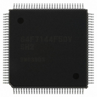
HD64F7144F50V
Manufacturer Part Number
HD64F7144F50V
Description
IC SUPERH MCU FLASH 256K 112QFP
Manufacturer
Renesas Electronics America
Series
SuperH® SH7144r
Specifications of HD64F7144F50V
Core Processor
SH-2
Core Size
32-Bit
Speed
50MHz
Connectivity
EBI/EMI, I²C, SCI
Peripherals
DMA, POR, PWM, WDT
Number Of I /o
74
Program Memory Size
256KB (256K x 8)
Program Memory Type
FLASH
Ram Size
8K x 8
Voltage - Supply (vcc/vdd)
3 V ~ 3.6 V
Data Converters
A/D 8x10b
Oscillator Type
Internal
Operating Temperature
-20°C ~ 75°C
Package / Case
112-QFP
For Use With
HS0005KCU11H - EMULATOR E10A-USB H8S(X),SH2(A)EDK7145 - DEV EVALUATION KIT SH7145
Lead Free Status / RoHS Status
Lead free / RoHS Compliant
Eeprom Size
-
Available stocks
Company
Part Number
Manufacturer
Quantity
Price
Company:

Part Number:
HD64F7144F50V
Manufacturer:
RENESAS
Quantity:
450
Company:
Part Number:
HD64F7144F50V
Manufacturer:
Renesas Electronics America
Quantity:
10 000
Part Number:
HD64F7144F50V
Manufacturer:
RENESAS/瑞萨
Quantity:
20 000


15. A/D Converter
15.3
The A/D converter has the following registers. For details on register addresses and register states
in each processing state, refer to section 25, List of Registers.
• A/D data register 0 (ADDR0)
• A/D data register 1 (ADDR1)
• A/D data register 2 (ADDR2)
• A/D data register 3 (ADDR3)
• A/D data register 4 (ADDR4)
• A/D data register 5 (ADDR5)
• A/D data register 6 (ADDR6)
• A/D data register 7 (ADDR7)
• A/D control/status register_0 (ADCSR_0)
• A/D control/status register_1 (ADCSR_1)
• A/D control register_0 (ADCR_0)
• A/D control register_1 (ADCR_1)
• A/D trigger select register (ADTSR)
15.3.1
ADDRs are 16-bit read-only registers. The conversion result for each analog input channel is
stored in ADDR with the corresponding number. (For example, the conversion result of AN4 is
stored in ADDR4.)
The converted 10-bit data is stored in bits 6 to 15. The lower 6 bits are always read as 0.
The data bus between the CPU and the A/D converter is 8 bits wide. The upper byte can be read
directly from the CPU, however the lower byte should be read via a temporary register. The
temporary register contents are transferred from the ADDR when the upper byte data is read.
When reading the ADDR, read the upper byte before the lower byte, or read in word unit.
The initial value of ADDR is H'0000.
Rev.4.00 Mar. 27, 2008 Page 544 of 882
REJ09B0108-0400
Register Descriptions
A/D Data Registers 0 to 7 (ADDR0 to ADDR7)
Related parts for HD64F7144F50V
Image
Part Number
Description
Manufacturer
Datasheet
Request
R


Part Number:
Description:
KIT STARTER FOR M16C/29
Manufacturer:
Renesas Electronics America
Datasheet:

Part Number:
Description:
KIT STARTER FOR R8C/2D
Manufacturer:
Renesas Electronics America
Datasheet:

Part Number:
Description:
R0K33062P STARTER KIT
Manufacturer:
Renesas Electronics America
Datasheet:

Part Number:
Description:
KIT STARTER FOR R8C/23 E8A
Manufacturer:
Renesas Electronics America
Datasheet:

Part Number:
Description:
KIT STARTER FOR R8C/25
Manufacturer:
Renesas Electronics America
Datasheet:

Part Number:
Description:
KIT STARTER H8S2456 SHARPE DSPLY
Manufacturer:
Renesas Electronics America
Datasheet:

Part Number:
Description:
KIT STARTER FOR R8C38C
Manufacturer:
Renesas Electronics America
Datasheet:

Part Number:
Description:
KIT STARTER FOR R8C35C
Manufacturer:
Renesas Electronics America
Datasheet:

Part Number:
Description:
KIT STARTER FOR R8CL3AC+LCD APPS
Manufacturer:
Renesas Electronics America
Datasheet:
Part Number:
Description:
KIT STARTER FOR RX610
Manufacturer:
Renesas Electronics America
Datasheet:

Part Number:
Description:
KIT STARTER FOR R32C/118
Manufacturer:
Renesas Electronics America
Datasheet:

Part Number:
Description:
KIT DEV RSK-R8C/26-29
Manufacturer:
Renesas Electronics America
Datasheet:

Part Number:
Description:
KIT STARTER FOR SH7124
Manufacturer:
Renesas Electronics America
Datasheet:

Part Number:
Description:
KIT STARTER FOR H8SX/1622
Manufacturer:
Renesas Electronics America
Datasheet: