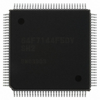
HD64F7144F50V Renesas Electronics America, HD64F7144F50V Datasheet - Page 677

HD64F7144F50V
Manufacturer Part Number
HD64F7144F50V
Description
IC SUPERH MCU FLASH 256K 112QFP
Manufacturer
Renesas Electronics America
Series
SuperH® SH7144r
Specifications of HD64F7144F50V
Core Processor
SH-2
Core Size
32-Bit
Speed
50MHz
Connectivity
EBI/EMI, I²C, SCI
Peripherals
DMA, POR, PWM, WDT
Number Of I /o
74
Program Memory Size
256KB (256K x 8)
Program Memory Type
FLASH
Ram Size
8K x 8
Voltage - Supply (vcc/vdd)
3 V ~ 3.6 V
Data Converters
A/D 8x10b
Oscillator Type
Internal
Operating Temperature
-20°C ~ 75°C
Package / Case
112-QFP
For Use With
HS0005KCU11H - EMULATOR E10A-USB H8S(X),SH2(A)EDK7145 - DEV EVALUATION KIT SH7145
Lead Free Status / RoHS Status
Lead free / RoHS Compliant
Eeprom Size
-
Available stocks
Company
Part Number
Manufacturer
Quantity
Price
Company:
Part Number:
HD64F7144F50V
Manufacturer:
RENESAS
Quantity:
450
Company:
Part Number:
HD64F7144F50V
Manufacturer:
Renesas Electronics America
Quantity:
10 000
Part Number:
HD64F7144F50V
Manufacturer:
RENESAS/瑞萨
Quantity:
20 000
- Current page: 677 of 932
- Download datasheet (6Mb)
17.2
1. In this LSI, the same function is available as a multiplexed function on multiple pins. This
Table 17.15 Transmit Forms of Input Functions Allocated to Multiple Pins
Note:
2. When the port input is switched from a low level to the DREQ or the IRQ edge for the pins
3. Do not set functions other than those specified in tables 17.13 and 17.14. Otherwise, correct
4. When pin functions are selected, set the port I/O registers (PBIOR and PDIORL) after setting
Product
SH7144
SH7145
approach is intended to increase the number of selectable pin functions and to allow the easier
design of boards. If two or more pins are specified for one function, however, there are two
cautions shown below.
⎯ When the pin function is input
⎯ When the pin function is output
that are multiplexed with input/output and DREQ or IRQ, the corresponding edge is detected.
operation cannot be guaranteed.
the port control registers (PBCR1, PBCR2, PDCRL1, and PDCRL2).
However, when selecting pin functions that are multiplexed with port A, port C, PD31 to PD16
of port D, and port E, no strict attention is required in setting the order of port control registers
(PACRH, PACRL1, PACRL2, PCCR, PDCRH1, PDCRH2, PECRL1, and PECRL2) and port
I/O registers (PAIORH, PAIORL, PCIOR, PDIORH, and PEIORL).
Signals input to several pins are formed as one signal through OR or AND logic and the
signal is transmitted into the LSI. Therefore, a signal that differs from the input signals may
be transmitted to the LSI depending on the input signals in other pins that have the same
functions. Table 17.15 shows the transmit forms of input functions allocated to several
pins. When using one of the functions shown below in multiple pins, use it with care of
signal polarity considering the transmit forms.
OR type: Signals input to several pins are formed as one signal through OR logic and the
AND type: Signals input to several pins are formed as one signal through AND logic and
Each selected pin can output the same function.
*
Usage Notes
F-ZTAT version only
signal is transmitted into the LSI.
the signal is transmitted into the LSI.
OR Type
SCK3, RXD3
SCK3, RXD3, AUDMD*,
AUDATA0 to AUDATA3*
Rev.4.00 Mar. 27, 2008 Page 631 of 882
AND Type
IRQ0 to IRQ3, DREQ0, DREQ1
IRQ0 to IRQ7, DREQ0, DREQ1,
BREQ, WAIT, ADTRG, AUDRST*,
AUDSYNC*, AUDCK*
17. Pin Function Controller (PFC)
REJ09B0108-0400
Related parts for HD64F7144F50V
Image
Part Number
Description
Manufacturer
Datasheet
Request
R

Part Number:
Description:
KIT STARTER FOR M16C/29
Manufacturer:
Renesas Electronics America
Datasheet:

Part Number:
Description:
KIT STARTER FOR R8C/2D
Manufacturer:
Renesas Electronics America
Datasheet:

Part Number:
Description:
R0K33062P STARTER KIT
Manufacturer:
Renesas Electronics America
Datasheet:

Part Number:
Description:
KIT STARTER FOR R8C/23 E8A
Manufacturer:
Renesas Electronics America
Datasheet:

Part Number:
Description:
KIT STARTER FOR R8C/25
Manufacturer:
Renesas Electronics America
Datasheet:

Part Number:
Description:
KIT STARTER H8S2456 SHARPE DSPLY
Manufacturer:
Renesas Electronics America
Datasheet:

Part Number:
Description:
KIT STARTER FOR R8C38C
Manufacturer:
Renesas Electronics America
Datasheet:

Part Number:
Description:
KIT STARTER FOR R8C35C
Manufacturer:
Renesas Electronics America
Datasheet:

Part Number:
Description:
KIT STARTER FOR R8CL3AC+LCD APPS
Manufacturer:
Renesas Electronics America
Datasheet:

Part Number:
Description:
KIT STARTER FOR RX610
Manufacturer:
Renesas Electronics America
Datasheet:

Part Number:
Description:
KIT STARTER FOR R32C/118
Manufacturer:
Renesas Electronics America
Datasheet:

Part Number:
Description:
KIT DEV RSK-R8C/26-29
Manufacturer:
Renesas Electronics America
Datasheet:

Part Number:
Description:
KIT STARTER FOR SH7124
Manufacturer:
Renesas Electronics America
Datasheet:

Part Number:
Description:
KIT STARTER FOR H8SX/1622
Manufacturer:
Renesas Electronics America
Datasheet:


